Review
. 2024 Feb 29;15(3):349.
doi: 10.3390/mi15030349.

Progress in Electronic, Energy, Biomedical and Environmental Applications of Boron Nitride and MoS2 Nanostructures

Affiliations
Review

Progress in Electronic, Energy, Biomedical and Environmental Applications of Boron Nitride and MoS2 Nanostructures

Join Uddin et al. Micromachines (Basel). .

Abstract

In this review, we examine recent progress using boron nitride (BN) and molybdenum disulfide (MoS2) nanostructures for electronic, energy, biomedical, and environmental applications. The scope of coverage includes zero-, one-, and two-dimensional nanostructures such as BN nanosheets, BN nanotubes, BN quantum dots, MoS2 nanosheets, and MoS2 quantum dots. These materials have sizable bandgaps, differentiating them from other metallic nanostructures or small-bandgap materials. We observed two interesting trends: (1) an increase in applications that use heterogeneous materials by combining BN and MoS2 nanostructures with other nanomaterials, and (2) strong research interest in environmental applications. Last, we encourage researchers to study how to remove nanomaterials from air, soil, and water contaminated with nanomaterials. As nanotechnology proceeds into various applications, environmental contamination is inevitable and must be addressed. Otherwise, nanomaterials will go into our food chain much like microplastics.

Keywords: biomedicine; boron nitride; electronics; energy; environment; molybdenum disulfide.


Conflict of interest statement

The authors declare no conflicts of interest.

Figures

Figure 1
Figure 1
Schematic illustration of the importance of studying the environmental application of nanomaterials. (1) Air pollution from nanotech activities will eventually bring pollutants to soil, lakes, rivers, oceans, and groundwater via processes (2) to (6). The unintentional contamination of water by nanomaterials during environmental application is highly possible. Therefore, research to purify water by extracting nanomaterials from water (7 and 8) becomes critical [9,10]. Credit: Y. K. Yap.
Figure 2
Figure 2
Schematic illustration of (a) BN and (b) MoS2 nanostructures. Credit: Y. K. Yap.
Figure 3
Figure 3
(a) Schematic illustration of Te-based FET with global bottom-gate structure on h-BN/SiO2/Si substrate in a cross-sectional view. (b) Field-effect mobility of Te transistor extracted from the transfer curves under the bias of Vd = 10 mV in the panel. (c) Schematic illustration of local bottom-gate Te FET by using h-BN as a dielectric layer in a cross-sectional view. (d) Field-effect mobility of Te transistor extracted from the transfer curve under the bias of Vd = 10 mV [30]. Reproduced with the permission of Springer (Copyright 2022).
Figure 4
Figure 4
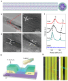
(a) Schematic illustration of a Te-BNNT. (b) TEM image of a 5 nm Te NW in a BNNT. (c) Enlarged HRTEM image of the region outlined in red in (b). (d,e) HRTEM images of BNNTs filled with 5 nm (d) and 2 nm (e) Te NWs. (f) Raman spectrum comparison of Te NWs in BNNTs with different diameters as indicated. (g) Schematic illustration of an individual Te-BNNT FET. (h) False-colored SEM image of a representative FET device before Al2O3 capping [25]. Reproduced with the permission of Springer Nature (Copyright 2020).
Figure 5
Figure 5
(a) Schematic and (b) cross-sectional SEM image of the Organic Photovoltaics with inverted device structure. (c) J–V curves without HTL and with MoO3, PEDOT: PSS, or h-BN. (d) Schematic and (e) cross-sectional SEM image of the OPV with conventional device structure and (f) J–V curves of the OPVs without HTL and with PEDOT: PSS or h-BN [38]. Reproduced with the permission of Wiley (Copyright 2021).
Figure 6
Figure 6
(a) SEM image. (b) EDX mapping of the BN/S/C sample. (c) Long-term repeated charge/discharge cycling measurements for BN/S/C at a current density of 100 mAg−1 within a potential window of 0.05–2.2 V vs. AlCl4/Al (d) MoS2/S/C and (e) WS2/S/C [53]. Reproduced with the permission of Springer Nature (Copyright 2019).
Figure 7
Figure 7
Illustration of an FET based on Bi/MoS2 contacts. The Bi (0001) plane is parallel to the plane of MoS2 [75]. (Credit: Massachusetts Institute of Technology).
Figure 8
Figure 8
TEM (left) and HRTEM (inset) images of the flower-like 3DG/MoS2. TEM image (upper right) of 3DG/MoS2 and the corresponding EDX elemental mapping of S, Mo, and C [93]. Reproduced with the permission of Elsevier (Copyright 2016).
Figure 9
Figure 9
(a) Schematic of the perovskite solar cell with MoS2 nanoflakes. (b) Energy band diagram of the device shows the function of MoS2 as an additional HTL [102]. Reproduced with the permission of Springer Nature (Copyright 2020).
Figure 10
Figure 10
(a) Normalized ECL intensity of sensor with different concentrations of DA (0, 0.5, 1, 10, 100, 300, 500, 800, 1000, 5000, 10000 μM). (b) Linear relationship between (I0 − I)/I0 and the natural logarithm concentration of DA in the range of 1−1000 μM [124]. Reproduced with the permission of America Chemical Society (Copyright 2018).
Figure 11
Figure 11
Schematic drawing of (a) a DSPE-PEG-NH linker with a FITC molecule to form a dye-linker. (b) Non-covalent functionalization scheme to conjugate dye-linkers on each BNNT [13]. Reproduced with the permission of Springer Nature (Copyright 2020).
Figure 12
Figure 12
Schematic illustration of the nanocarriers (M-MoS2/MMA-G 5/L-A/PVE) [142]. Reproduced with the permission of Wiley (Copyright 2021).
Figure 13
Figure 13
Schematic illustration of the synthesis of JR400-MoS2 NPs, drug (ATE) loading, and in vitro skin penetration experiments. Inset: SEM image of one NP [145]. Reproduced with the permission of Taylor and Francis (Copyright 2020).
Figure 14
Figure 14
Schematic illustration of a colorimetric sensor based on MoS2Au@Pt nanocomposites [146]. Reproduced with the permission of America Chemical Society (Copyright 2022).
Figure 15
Figure 15
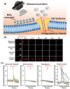
(a) Schematic illustration of the underlying mechanism. (b) Time-lapse Ca2+ images of the neuron cells upon different stimulation conditions. (c) Time course of ΔF/F0. Data are obtained from three to six independent experiments [147]. Reproduced with the permission of America Chemical Society (Copyright 2023).
Figure 16
Figure 16
(a) Tumor changes during 14 days of PBS, MDMP, and MDMP + NIR treatment. (b) Tumor size map after the treatment of PBS, MDMP, and MDMP + NIR. (c) Tumor weight after the treatment of PBS, MDMP, and MDMP + NIR. (d) Body weight changes of mice during 14 days of treatment by PBS, MDMP, and MDMP + NIR [148]. Reproduced with the permission of America Chemical Society (Copyright 2022).
Figure 17
Figure 17
The salt rejection (green bars) and water permeation (blue bars) in BNNT at various chiralities [(5,5) in (a), (6,6) in (b), (7, 7) in (c), and (8,8) in (d)] and applied pressures [159]. Reproduced with the permission of the Royal Society of Chemistry (Copyright 2017).
Figure 18
Figure 18
(a) Water flux rate and salt rejection of (b) Na+ and (c) Cl of each system under different pressures [162]. Reproduced with the permission of Elsevier (Copyright 2023).
Figure 19
Figure 19
Schematic of the sensor (left), transient resistance curves of NO2 gas sensing on MoS2:2D−QC nanocomposite sensors at 100 °C (upper right), and the selectivity responses of MoS2 and MoS2:2D−QC nanocomposite sensors (bottom right) [182]. Reproduced with the permission of America Chemical Society (Copyright 2023).

References

    1. Ekimov A.I., Onushchenko A.A. Quantum size effect in 3-dimensional microscopic semiconductor crystals. JETP Lett. 1981;34:345–349. doi: 10.1134/S0021364023130040. - DOI
    1. Brus L.E. Electron–electron and electron-hole interactions in small semiconductor crystallites: The size dependence of the lowest excited electronic state. J. Chem. Phys. 1984;80:4403–4409. doi: 10.1063/1.447218. - DOI
    1. Murray C.B., Norris D.J., Bawendi M.G. Synthesis and characterization of nearly monodisperse CdE (E = sulfur, selenium, tellurium) semiconductor nanocrystallites. J. Am. Chem. Soc. 1993;115:8706–8715. doi: 10.1021/ja00072a025. - DOI
    1. Iijima S. Helical microtubules of graphitic carbon. Nature. 1991;354:56–58. doi: 10.1038/354056a0. - DOI
    1. Roco M.C., Williams R.S., Alivisatos P. Vision for Nanotechnology in the Next Decade. Springer; Dordrecht, The Netherlands: 2000. Nanotechnology Research Directions: IWGN Workshop Report.