

The Effect of Pixel Design and Operation Conditions on Linear Output Range of 4T CMOS Image Sensors
- PMID: 38544103
- PMCID: PMC10975077
- DOI: 10.3390/s24061841
The Effect of Pixel Design and Operation Conditions on Linear Output Range of 4T CMOS Image Sensors
Abstract
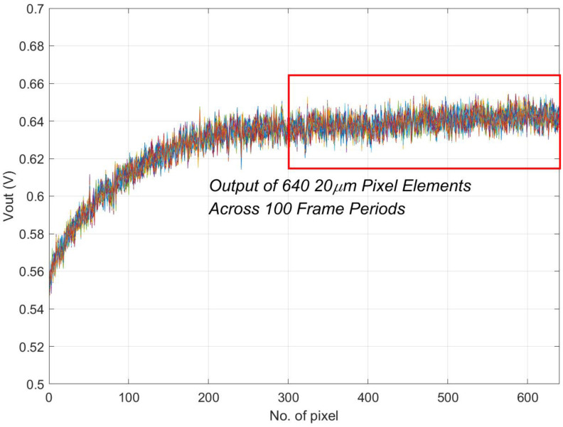
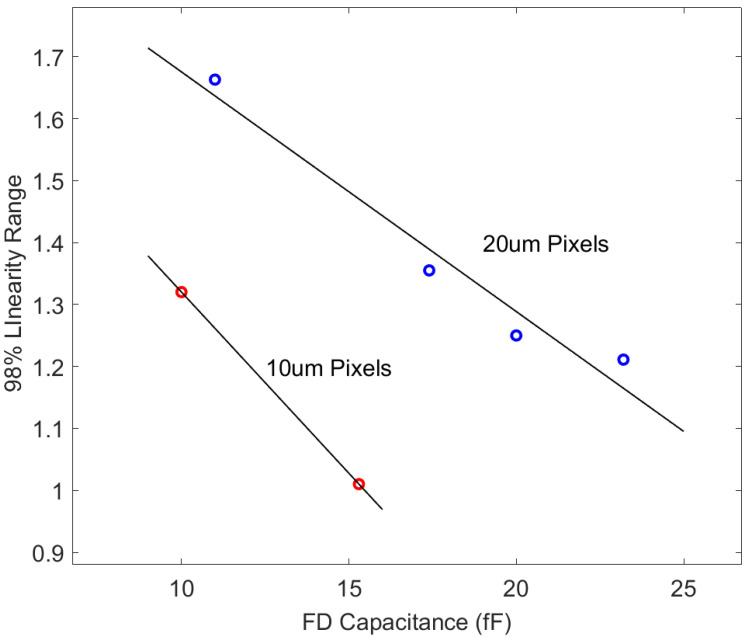
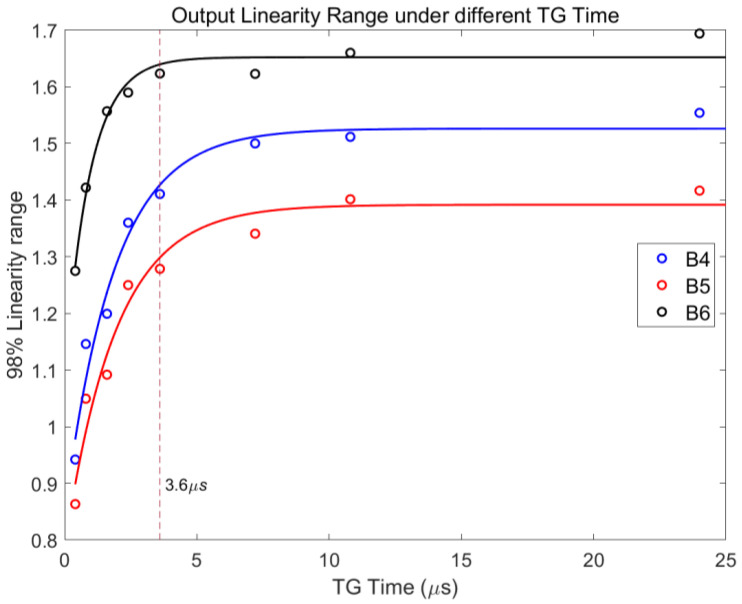
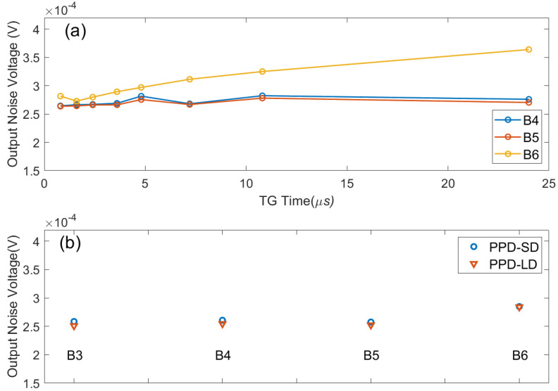
We analyze several factors that affect the linear output range of CMOS image sensors, including charge transfer time, reset transistor supply voltage, the capacitance of integration capacitor, the n-well doping of the pinned photodiode (PPD) and the output buffer. The test chips are fabricated with 0.18 μm CMOS image sensor (CIS) process and comprise six channels. Channels B1 and B2 are 10 μm pixels and channels B3-B6 are 20 μm pixels, with corresponding pixel arrays of 1 × 2560 and 1 × 1280 respectively. The floating diffusion (FD) capacitance varies from 10 fF to 23.3 fF, and two different designs were employed for the n-well doping in PPD. The experimental results indicate that optimizing the FD capacitance and PPD design can enhance the linear output range by 37% and 32%, respectively. For larger pixel sizes, extending the transfer gate (TG) sampling time leads to an increase of over 60% in the linear output range. Furthermore, optimizing the design of the output buffer can alleviate restrictions on the linear output range. The lower reset voltage for noise reduction does not exhibit a significant impact on the linear output range. Furthermore, these methods can enhance the linear output range without significantly amplifying the readout noise. These findings indicate that the linear output range of pixels is not only influenced by pixel design but also by operational conditions. Finally, we conducted a detailed analysis of the impact of PPD n-well doping concentration and TG sampling time on the linear output range. This provides designers with a clear understanding of how nonlinearity is introduced into pixels, offering valuable insight in the design of highly linear pixels.
Keywords: 4-Transistor; CMOS image sensor; linear output range; operation conditions; pixel design.
Conflict of interest statement
The authors declare no conflicts of interest.
Figures


References
-
- Fossum E.R., Hondongwa D.B. A review of the pinned photodiode for CCD and CMOS image sensors. IEEE J. Electron Devices Soc. :2014. doi: 10.1109/JEDS.2014.2306412. - DOI
-
- Stevens M., Párraga C.A., Cuthill I.C., Partridge J.C., Troscianko T.S. Using digital photography to study animal coloration. Biol. J. Linn. Soc. 2007;90:211–237. doi: 10.1111/j.1095-8312.2007.00725.x. - DOI
-
- Brunetti A.M., Choubey B. A low dark current 160 dB logarithmic pixel with low voltage photodiode biasing. Electronics. 2021;10:1096. doi: 10.3390/electronics10091096. - DOI
-
- Storm G., Henderson R., Hurwitz J., Renshaw D., Findlater K., Purcell M. Extended dynamic range from a combined linear-logarithmic CMOS image sensor. IEEE J. Solid-State Circuits. 2006;41:2095–2106. doi: 10.1109/JSSC.2006.880613. - DOI
-
- Wang F., Han L., Theuwissen A.J.P. Development and evaluation of a highly linear CMOS image sensor with a digitally assisted linearity calibration. IEEE J. Solid-State Circuits. 2018;53:2970–2981. doi: 10.1109/JSSC.2018.2856252. - DOI
Grants and funding
LinkOut - more resources
Full Text Sources
Miscellaneous
