Review
. 2024 Feb 27;11(3):816-865.
doi: 10.1021/acsphotonics.3c00457. eCollection 2024 Mar 20.

Roadmap for Optical Metasurfaces

Affiliations
Review

Roadmap for Optical Metasurfaces

Arseniy I Kuznetsov et al. ACS Photonics. .

Abstract

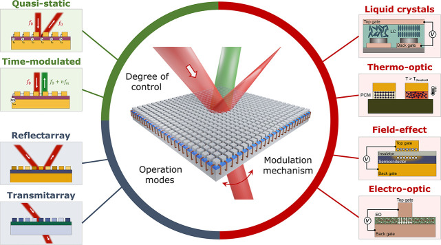
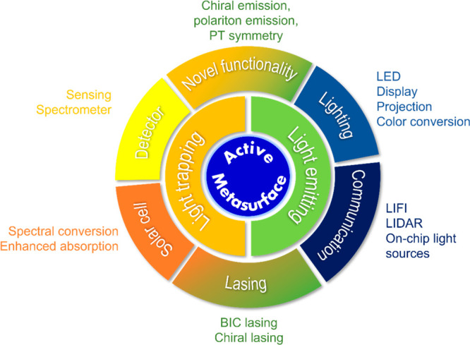
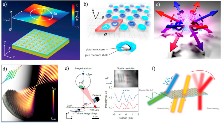
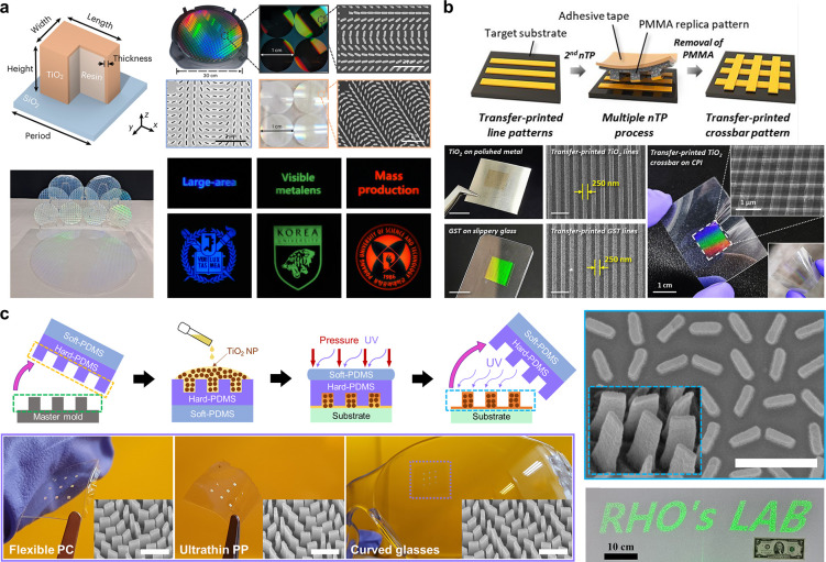
Metasurfaces have recently risen to prominence in optical research, providing unique functionalities that can be used for imaging, beam forming, holography, polarimetry, and many more, while keeping device dimensions small. Despite the fact that a vast range of basic metasurface designs has already been thoroughly studied in the literature, the number of metasurface-related papers is still growing at a rapid pace, as metasurface research is now spreading to adjacent fields, including computational imaging, augmented and virtual reality, automotive, display, biosensing, nonlinear, quantum and topological optics, optical computing, and more. At the same time, the ability of metasurfaces to perform optical functions in much more compact optical systems has triggered strong and constantly growing interest from various industries that greatly benefit from the availability of miniaturized, highly functional, and efficient optical components that can be integrated in optoelectronic systems at low cost. This creates a truly unique opportunity for the field of metasurfaces to make both a scientific and an industrial impact. The goal of this Roadmap is to mark this "golden age" of metasurface research and define future directions to encourage scientists and engineers to drive research and development in the field of metasurfaces toward both scientific excellence and broad industrial adoption.


Conflict of interest statement

The authors declare no competing financial interest.

Figures

Figure 1
Figure 1
Road ahead for optical metasurfaces.
Figure 2
Figure 2
Concepts, implementations, and applications of meta-lenses. Full-color routing: Reproduced with permission from ref (13). Copyright 2017 American Chemical Society. Achromatic imaging: Reproduced with permission from ref (14). Copyright 2018 Springer Nature. Biomedical imaging: Reproduced with permission from ref (15). Copyright 2021 American Chemical Society. Edge detection: Reproduced with permission from ref (18). Copyright 2021 De Gruyter. Phase sensing: Reprinted or adapted with permission under a Creative Commons CC-BY 4.0 from ref (19). Copyright 2021 Springer Nature. Polarization detection: Reproduced with permission from ref (20). Copyright 2018 American Chemical Society. Nonlinear generation: Reprinted or adapted with permission under a Creative Commons CC-BY 4.0 from ref (22). Copyright 2022 American Association for the Advancement of Science. Quantum source: Reproduced with permission from ref (23). Copyright 2020 American Association for the Advancement of Science.
Figure 3
Figure 3
Measuring picometer nanowire displacements via scattering of topologically structured light (following ref (39)). Incident light is topologically structured. Light scattered from the 100 nm wide nanowire is mapped in transmission through a high-NA microscope objective (not shown). Deeply subwavelength lateral (x-direction) displacements of the wire, controlled by application of a DC bias between the wire and the adjacent edge of the supporting membrane, are quantified via a deep-leaning enabled analysis of single-shot scattering patterns.
Figure 4
Figure 4
(a) Schematic of wavelength multiplexing where the metasurface imposes different transformations for different wavelengths (colors). (b) Polarization multiplexing where the transformation is different depending on the polarization. (c) Angular multiplexing where wavefronts incident at different angles experience very different transformations.
Figure 5
Figure 5
Spectral amplitude control: future of color coatings, high-density information carriers, and miniaturized spectrometers and displays. (a) Categories of nanostructures interacting with incident white light to generate color. (b.1) Advantages of photonic surface colorants over traditional dyes. (b.2) Self-assembled Al particles on the Al2O3-coated Al mirror to generate angle and polarization-independent structural color. (b.3) Mass production of structurally colored Al/Al2O3/Al and cellulose pigments, scalebar 1 cm. (c.1) Gold nanorod-based 5D optical recording with polarization, wavelength, and space, scalebar 100 μm; multiple images stored in one structure made of Al nanoantenna and revealed with polarizer and analyzer, scalebar 40 μm; gap-plasmon resonator-based color print at the optical diffraction limit, scalebar left 1 μm, middle and right 500 nm. (c.2) Reconfigurable structural colors with 3D printed shape memory gratings, scalebar 1 μm in SEM image and 40 μm in the optical image; three holographic images hidden in one color print with 3D printed nanopillars on phase plate structures, scalebar 200 μm; colorful benchy made of 3D printed woodpile photonic crystals with different parameters, scalebar 30 μm. (c.3) Optical authentication with a physical unclonable function (PUF). (d.1) Photograph of structurally colored silicon nanowire microspectrometer with 5 mm scale bar, middle shows bright field optical microscopic image of the center of device, scalebar 200 μm, the colorful texts and palettes are made of nanowires with different radii, scalebar 1 μm. Photocurrent value from each photodetector forms an initial data cube and a spectral data cube can be obtained from the photocurrent data cube to reconstruct the spectrum using different algorithms. (d.2) Schematics of the operating principle of a 2D extrinsic chiral metasurface, 3D intrinsic chiral metamaterial, and optically thick planar structure with intrinsic chirality under their respective illumination conditions. (d.3) Microscopic images of a colorful Afghan Girl image with different electric fields applied on the reflective plasmonic-liquid crystal display, scalebar top 100 μm, bottom left 20 μm, bottom right 150 nm; schematic of a universal photonic pixel consisting of two color-tunable elements and a top transmission-tunable layer. Right of (b.3) adapted with permission from ref (71). Copyright 2022. Top of (c.1) adapted with permission from ref (72). Copyright 2009. bottom of (c.1) adapted with permission from ref (73). Copyright 2012. Left top of (c.2) adapted with permission under a Creative Commons CC-BY 4.0 from ref (75). Copyright 2021. Left bottom of (c.2) adapted with permission under a Creative Commons CC-BY 4.0 from ref (76). Copyright 2019. (d.2) adapted with permission under a Creative Commons CC-BY 4.0 from ref (82). Copyright 2018. Left of (d.3) adapted with permission under a Creative Commons CC-BY 4.0 from ref (83). Copyright 2015 Nature Publishing Group. Middle of (c.1) adapted with permission from ref (74). Copyright 2021 Wiley-VCH Verlag GmbH & Co. KGaA, Weinheim. Right of (c.2) adapted with permission from ref (77). Copyright 2022. Top of (d.1) adapted with permission from ref (78). Copyright 2019. Right of (d.3) adapted with permission from ref (84). Copyright 2020 American Chemical Society.
Figure 6
Figure 6
(a) A typical example of a multilayer meta-optic made of plasmonic nanoresonators separated with precise spacing using a spin-on-glass dielectric material. (b) 3D focused ion-beam milling of a v-shaped plasmonic metasurface stack utilized for efficient backward second harmonic generation. (c) Stacking metasurfaces to form a bilayer optical component, in this case, an edge imager. (d) Two-layer metasurfaces separated by a large distance and large energy redistribution for achieving lenses with low coma aberration. (e) A hybrid optical system composed of a refractive and a diffractive meta-optic designed for chromatic aberration correction. (f) A stack of transversely and longitudinally phase matched metasurfaces to achieve arbitrary nonlinear light manipulation capabilities. (a), (b), and (f) have been reproduced or adapted with permission from ref (94). Copyright 2021 APS.
Figure 7
Figure 7
Conceptual framework for the freeform design of a large area, multiscalar metasurface. The desired function is framed as a Figure of Merit and the metasurface layout is optimized over a series of iterations in a manner that maximizes the Figure of Merit. During each iteration, pairs of electromagnetic simulations (i.e., “forward” and “adjoint” simulations) are performed to compute gradients that specify how perturbative changes to the dielectric constant everywhere in the device can improve device performance. Algorithms (i.e., NLopt, MathWorks, scipy, GLOnet) specify the detailed utilization of gradient calculations in the optimization process.
Figure 8
Figure 8
By optimizing meta-optics, along with a computational backend, a dramatic reduction in size, weight, power, and latency of image sensors can be achieved. Here, we consider four examples, where the objects are shown in the left and desired sensing output is shown in the left. We envision the computational sensors can either capture aesthetically pleasing images (row 1), or capture additional information from the scene, such as depth (row 2) or spectrum. We envision that some of these can even perform computation for object detection (row 3) or scene understanding (row 4).
Figure 9
Figure 9
Metasurfaces for optical computing and signal processing: (a) Sketch of the idea of metasurface that can perform mathematical operation on the profile of the incoming wave. Reprinted with permission from ref (133). Copyright 2014 AAAS. (b) Numerical demonstration of edge detection using the metasurface designed to perfrom the second-order spatial differentiation. Reprinted with permission from ref (133). Copyright 2014 AAAS. (c) Nonlocal metasurface using an array of split-ring resonator. Reprinted with permission from ref (134). Copyright 2018 American Physical Society. (d) the scanning electron mictroscopy (SEM) image of the Si metasurface performing second-order spatial differentiation, Reprinted from ref (135). Creative Common License, Copyright 2019 American Chemical Society. (e) Experimental second-order image differentiation using the structure shown in (d). Reprinted from ref (135). Creative Common License, Copyright 2019 American Chemical Society. (f) Sketch of the idea of inverse-designed metastructure with the feedback for solving integral equations, Reprinted with permission from ref (137). Copyright 2019 AAAS. (g) The specific metastructure designed for experimental verification for integral equation solving. Reprinted with permission from ref (137). Copyright 2019 AAAS. (h) The photograph of the structure. Reprinted with permission from ref (137). Copyright 2019 AAAS. (i) From ref (138): Schematic on integral-solving metasurface geometry and scanning electron microscopy (SEM) image of an inverse-designed Si metagrating for equation solving with free-space visible radiation. Reprinted with permission from ref (138). Copyright 2023 Springer Nature.
Figure 10
Figure 10
Active metasurface configurations (left) and physical mechanisms for modulation (right).
Figure 11
Figure 11
Research directions and applications of active metasurfaces.
Figure 12
Figure 12
(a) Schematic of nonlinear frequency conversion effects. (b) Nonlinear emission spectrum of a GaAs metasurface dually pumped at the electric dipole and magnetic dipole modes. Scale bar in SEM image, 3 μm. The energy level diagrams of the measured frequency conversion processes are exhibited at the bottom. (c) Frequency tripling in a GaAs metasurface through a cascaded two-step second-order process, schematized on the left side of the figure. (d) High-harmonic generation in a GaP metasurface excited at the electric dipole resonance. The eighth harmonic was not registered due to light absorption of the dielectric at the radiation wavelength. (e) Diatomic metallic metasurface for SHG image encoding in the real and Fourier spaces using the PB phase principle. Scale bar in SEM image, 500 nm. (f) Representation of light-induced time-dependent refractive index (and resonance frequency) changes in a metasurface cavity. (g) Effective refractive index modulation measured in a ITO/Au hybrid metasurface excited at ITO’s epsilon-near-zero region. Scale bar in SEM image, 1 μm. (h) Transmission pump−probe measurement of a Si metasurface showing sub-100 fs modulation response due to two-photon absorption. (i) Schematic and nonlinear emission spectrum of a Si metasurface excited at different fluences at a wavelength of 3.62 μm. The signal of an unstructured reference film excited at the highest fluence is also included. MS stands for metasurface. Scale bar in SEM image, 1 μm. (a, b) Adapted with permission under a Creative Commons CC-BY 4.0 license from ref (177). Copyright 2018 Springer Nature. (c) Adapted with permission from ref (178). Copyright 2022 American Chemical Society. (d) Adapted with permission under a Creative Commons CC-BY 4.0 license from ref (179). Copyright 2021 Springer Nature. (e) Adapted with permission from ref (180). Copyright 2020 American Chemical Society. (f, i) Adapted with permission under a Creative Commons CC-BY 4.0 license from ref (181). Copyright 2019 Springer Nature. (g) Adapted with permission from ref (182). Copyright 2018 Springer Nature. (h) Adapted with permission from ref (183). Copyright 2015 American Chemical Society.
Figure 13
Figure 13
(a) This metasurface routes M input ports in state ψin to M output ports in state ψout allowing for quantum state reconstruction. Adapted with permission from ref (191). Copyright 2018 American Association for the Advancement of Science (AAAS). (b) Single-photon emitters in 2D hexagonal boron nitride (hBN) placed atop a high-quality plasmonic nanocavity array exhibit enhanced emission rates compared to single photon emitters in hBN placed on an unpatterned substrate. Adapted with permission from ref (193). Copyright 2017 the American Chemical Society (ACS). (c) Spontaneous parametric down conversion (SPDC) using symmetry-protected quasi-BIC resonances in a semiconductor metasurface. Adapted with permission from ref (194). Copyright 2022 American Association for the Advancement of Science (AAAS). (d) (Left) Setup of 2D array of dense atoms (with lattice constant a < wavelength λ) with reflected light. (Right) Band structure diagram for cooperative array (different colors denote the different polarizations; the dashed purple line is for circularly polarized light). The inset shows the Brillouin zone. Adapted with permission from ref (195). Copyright 2017 the American Physical Society.
Figure 14
Figure 14
(a) Topological metasurface for phase control around a singularity. Reproduced with permission from ref (205). Copyright 2021 AAAS. (b, c) Non-Hermitian metasurface to enhance the control over laser emission (b, geometry; c, chiral emission control). Adapted with permission under a Creative Commons CC-BY 4.0 from ref (209). Copyright 2021 American Physical Society. (d) Nonlocal metasurface to manipulate thermal emission. Reproduced from ref (159). Copyright 2022 Wiley. (e) Nonlocal metasurface for eyetracking applications. Reproduced with permission from ref (210). Copyright 2021 Nature Publishing Group. (f) Spatio-temporally modulated metasurface to extend the degree of control over wavefront manipulation to space-time diffraction. Reproduced with permission from ref (212). Copyright 2019 AAAS.
Figure 15
Figure 15
(a) Schematic of a high-n meta-atom with TiO2-coated NIL resin, Photograph and SEM images of the fabricated 12-in. master mold and replicated metasurfaces by NIL process, Fabricated 1 cm diameter metalens on glass wafers with various sizes, Photograph of virtual imaging by fabricated large-area metalens in red, green, blue wavelengths. Reprinted with permission from ref (237). Copyright 2023 Springer Nature. (b) Schematic of a thermally assisted nanotransfer printing process, a photograph of the transferred patterns on various substrates such as metal, glass, and flexible polyimide, and scanning electron microscope (SEM) images proving the high resolution of T-nTP for both metals and dielectrics including Ge2Se2Te5 (GST). All scale bars of SEM images in (b) are 1 μm. Reprinted with permission from ref (241). Copyright 2023 MDPI. (c) Schematic of a NIL process using high refractive index a TiO2 nanoparticle embedded resin, SEM images of the high-aspect-ratio metasurface, photographs of metasurfaces on various flexible substrates, and a high-efficiency holographic image. All scale bars of SEM images in (c) are 1 μm. Reprinted with permission from ref (244). Copyright 2022 Wiley-VCH GmbH.
Figure 16
Figure 16
Examples of first generation optical metasurface products and future estimation. (a) KolourOptik Stripe on a banknote, demonstrating 3D depth, using plasmonic nanostructures created on the contoured surfaces and interstitial bases of dome-shaped microstructures. Comparison of (b) traditional microlens and (c) META’s KolourOptik technology (https://blog.metamaterial.com/the-kolouroptik-platform). (d) A 12” wafer from a standard semiconductor foundry with 10000 lenses (Permission Metalenz, https://metalenz.com/metalenz-launches-its-metasurface-optics-on-the-open-market-in-partnership-with-umc/). (e) Space-saving and compact dot projectors with multifunctional meta-optics (https://metalenz.com/orion-pattern-projectors/). (f) Beam steering LiDARs (Permission Lumotive). (g) Growth of the number of metasurfaces on the market each year with increasing deployment of new metasurface technology, which enables new applications

References

    1. Yu N.; Capasso F. Flat Optics with Designer Metasurfaces. Nature Mat. 2014, 13, 139–150. 10.1038/nmat3839. - DOI - PubMed
    1. Kildishev A. V.; Boltasseva A.; Shalaev V. M. Planar photonics with metasurfaces. Science 2013, 339, 1232009. 10.1126/science.1232009. - DOI - PubMed
    1. Kuznetsov A. I.; Miroshnichenko A. E.; Brongersma M. L.; Kivshar Y. S.; Luk’yanchuk B. Optically Resonant Dielectric Nanostructures. Science 2016, 354, aag2472. 10.1126/science.aag2472. - DOI - PubMed
    1. Glybovski S. B.; Tretyakov S. A.; Belov P. A.; Kivshar Y. S.; Simovski C. R. Metasurfaces: From Microwaves to Visible. Phys. Rep. 2016, 634, 1–72. 10.1016/j.physrep.2016.04.004. - DOI
    1. Lalanne P.; Chavel P. Metalenses at Visible Wavelengths: Past, Present, Perspectives. Laser Photon. Rev. 2017, 11, 1600295. 10.1002/lpor.201600295. - DOI

LinkOut - more resources