

Resonant Raman Scattering Study of Strain and Defects in Chemical Vapor Deposition Grown MoS2 Monolayers
- PMID: 38558523
- PMCID: PMC12272025
- DOI: 10.1002/smll.202310685
Resonant Raman Scattering Study of Strain and Defects in Chemical Vapor Deposition Grown MoS2 Monolayers
Abstract
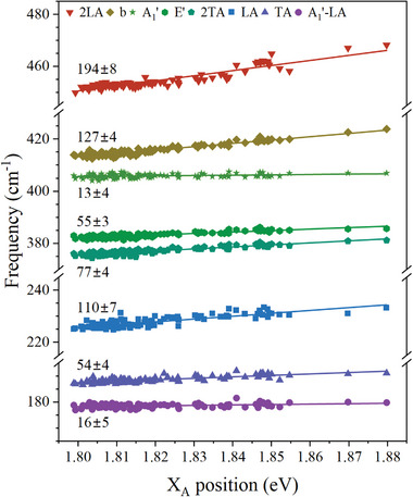
The development of bottom-up synthesis routes for semiconducting transition metal dichalcogenides (TMDs) and the assessment of their defects are of paramount importance to achieve their applications. TMD monolayers grown by chemical vapor deposition (CVD) can be subjected to significant strain and, here, Raman and photoluminescence spectroscopies are combined to characterize strain in over one hundred MoS2 monolayer samples grown by CVD. The frequency changes of phonons as a function of strain are analyzed, and used to extract the Grüneisen parameter of both zone-center and edge phonons. Additionally, the intensity of the defect-induced longitudinal acoustic (LA) and transverse acoustic (TA) Raman bands are discussed in relation to strain and electronic doping. The experimental mode-Grüneisen parameters obtained are compared with those calculated by density functional theory (DFT), to better characterize the type of strain and its resulting effects on Grüneisen parameters. The findings indicate that the use of Raman spectra to determine defect densities in 2D MoS2 must be always conducted considering strain effects. To the best of the authors' knowledge, this work constitutes the first report on double resonance Raman processes studied as a function of strain in 2D-MoS2. The new approach to obtain the Grüneisen parameter from zone-edge phonons in MoS2 can also be extended to other 2D semiconducting TMDs.
Keywords: 2D materials; DFT calculations; MoS2; Raman; chemical vapor deposition; defects; electronic doping; strain.
© 2024 The Authors. Small published by Wiley‐VCH GmbH.
Conflict of interest statement
The authors declare no conflict of interest.
Figures


References
-
- Splendiani A., Sun L., Zhang Y., Li T., Kim J., Chim C.‐Y., Galli G., Wang F., Nano Lett. 2010, 10, 1271. - PubMed
-
- Mak K. F., Lee C., Hone J., Shan J., Heinz T. F., Phys. Rev. Lett. 2010, 105, 136805. - PubMed
-
- Zhu Z. Y., Cheng Y. C., Schwingenschlögl U., Phys. Rev. B 2011, 84, 153402.
-
- Perea‐López N., Elías A. L., Berkdemir A., Castro‐Beltran A., Gutiérrez H. R., Feng S., Lv R., Hayashi T., López‐Urías F., Ghosh S., Muchharla B., Talapatra S., Terrones H., Terrones M., Adv. Funct. Mater. 2013, 23, 5511.
-
- Zeng H., Dai J., Yao W., Xiao D., Cui X., Nat. Nanotechnol. 2012, 7, 490. - PubMed
LinkOut - more resources
Full Text Sources
