

A 26-28 GHz, Two-Stage, Low-Noise Amplifier for Fifth-Generation Radio Frequency and Millimeter-Wave Applications
- PMID: 38610448
- PMCID: PMC11014129
- DOI: 10.3390/s24072237
A 26-28 GHz, Two-Stage, Low-Noise Amplifier for Fifth-Generation Radio Frequency and Millimeter-Wave Applications
Abstract
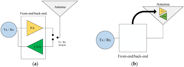
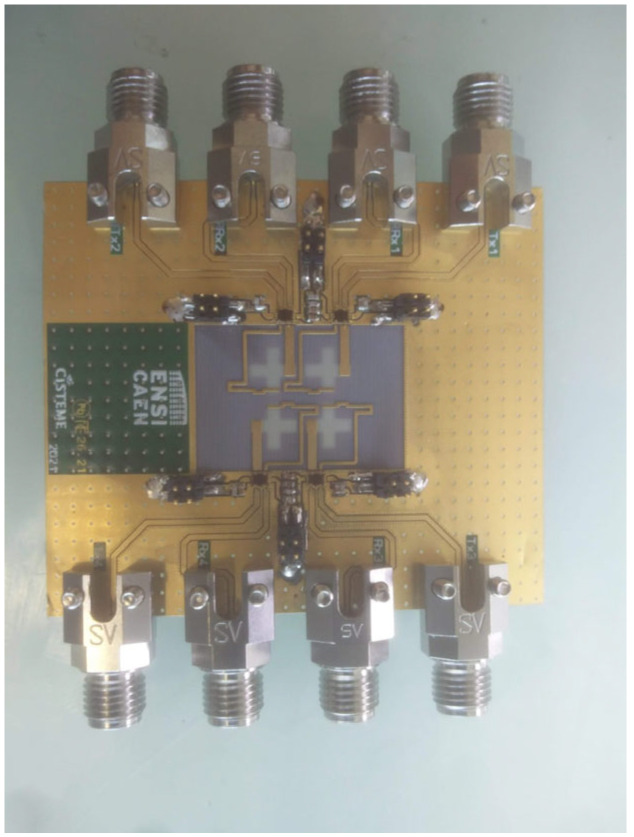
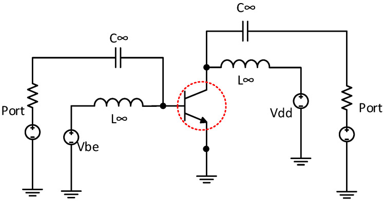
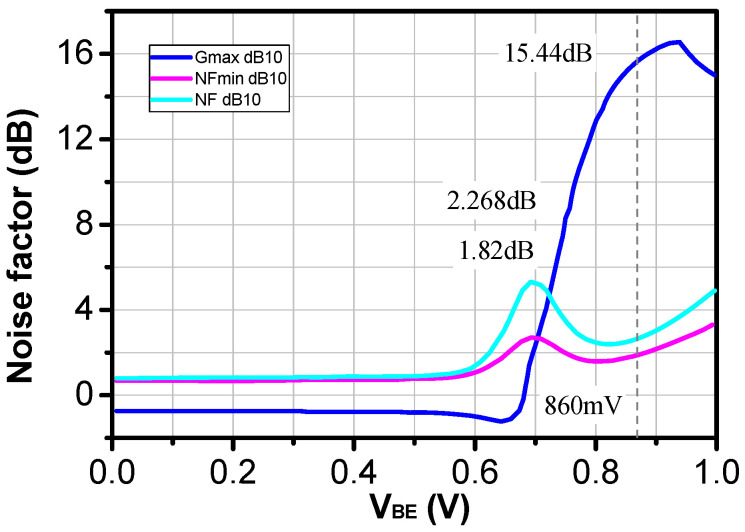
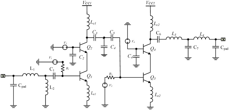
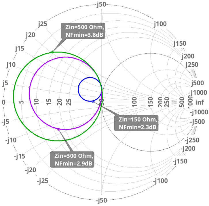
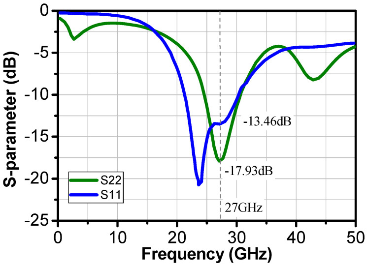
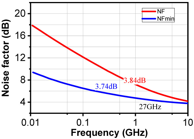
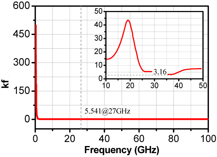
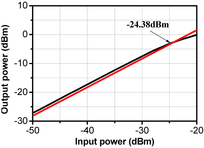
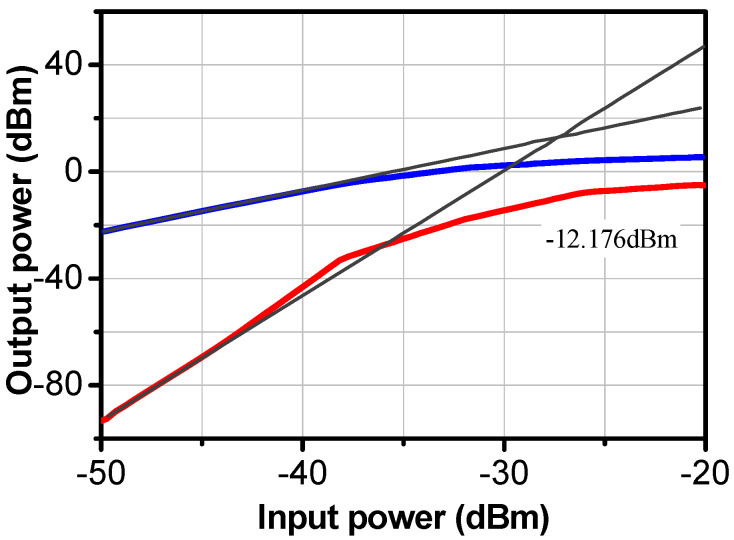
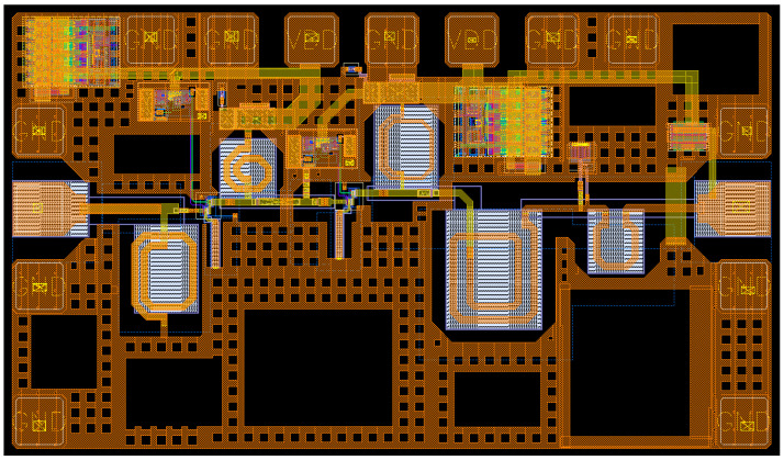
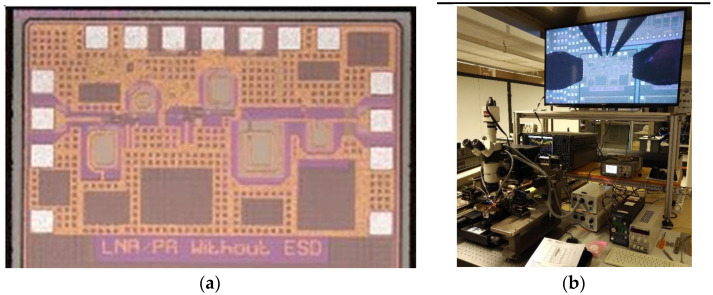
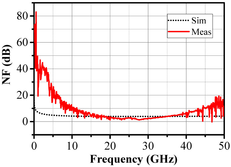
This paper presents a high-gain low-noise amplifier (LNA) operating at the 5G mm-wave band. The full design combines two conventional cascode stages: common base (CB) and common emitter (CS). The design technique reduces the miller effect and uses low-voltage supply and low-current-density transistors to simultaneously achieve high gain and low noise figures (NFs). The two-stage LNA topology is analyzed and designed using 0.25 µm SiGe BiCMOS process technology from NXP semiconductors. The measured circuit shows a small signal gain at 26 GHz of 26 dB with a gain error below 1 dB on the entire frequency band (26-28 GHz). The measured average NF is 3.84 dB, demonstrated over the full frequency band under 15 mA current consumption per stage, supplied with a voltage of 3.3 V.
Keywords: SiGe BiCMOS; cascode; fifth-generation mm-wave; low-noise amplifier; noise figure.
Conflict of interest statement
The authors declare that they have no conflicts of interest. All authors confirm that they have no conflicts of interest between themselves or with the party sponsoring this work.
Figures


References
-
- Geha C., Nguyen C., Silva-Martinez J. A Wideband Low-Power-Consumption 22–32.5-GHz 0.18-µm BiCMOS Active Balun-LNA With IM2 Cancellation Using a Transformer-Coupled Cascode-Cascade Topology. IEEE Trans. Microw. Theory Tech. 2017;65:536–547. doi: 10.1109/TMTT.2016.2623778. - DOI
-
- System Profiles for 10–66 GHz. Federal Communications Commission (FCC); Washington, DC, USA: 2002.
-
- Technical Requirements for Vehicular Radar Systems. Federal Communications Commission (FCC); Washington, DC, USA: 2002.
-
- Chen Z., Gao H., Leenaerts D.M.W., Milosevic D., Baltus P.G.M. A 16–43 GHz low-noise amplifier with 2.5–4.0 dB noise figure; Proceedings of the 2016 IEEE Asian Solid-State Circuits Conference (A-SSCC); Toyama, Japan. 7–9 November 2016.
-
- Gungor B., Turkmen E., Yazici M., Kaynak M., Gurbuz Y. 0.13μm SiGe BiCMOS W-Band Low-Noise Amplifier for Passive Imaging Systems; Proceedings of the 2018 18th Mediterranean Microwave Symposium (MMS); Istanbul, Turkey. 31 October–2 November 2018; Piscataway, NJ, USA: IEEE; 2019. pp. 206–209.
LinkOut - more resources
Full Text Sources
Miscellaneous
