. 2024 May 1;24(17):5110-5116.
doi: 10.1021/acs.nanolett.3c04460. Epub 2024 Apr 16.

Characterization of the Edge States in Colloidal Bi2Se3 Platelets

Affiliations

Characterization of the Edge States in Colloidal Bi2Se3 Platelets

Jesper R Moes et al. Nano Lett. .

Abstract

The remarkable development of colloidal nanocrystals with controlled dimensions and surface chemistry has resulted in vast optoelectronic applications. But can they also form a platform for quantum materials, in which electronic coherence is key? Here, we use colloidal, two-dimensional Bi2Se3 crystals, with precise and uniform thickness and finite lateral dimensions in the 100 nm range, to study the evolution of a topological insulator from three to two dimensions. For a thickness of 4-6 quintuple layers, scanning tunneling spectroscopy shows an 8 nm wide, nonscattering state encircling the platelet. We discuss the nature of this edge state with a low-energy continuum model and ab initio GW-Tight Binding theory. Our results also provide an indication of the maximum density of such states on a device.

Keywords: Bismuth selenide nanoplatelets; Density functional theory; Edge state; Quantum spin Hall insulator; Scanning tunneling spectroscopy; Topological insulator.


Conflict of interest statement

The authors declare no competing financial interest.

Figures
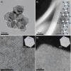
Figure 1
Figure 1
Structural characterization of colloidal Bi2Se3 NPLs. (A) TEM image of an ensemble of typical Bi2Se3 NPLs. (B) HAADF-STEM image with the viewing direction along the NPL, showing two NPLs consisting of 3 and 4 QLs, respectively. The two high intensity lines in each QL are due to the Bi columns (see inset). (C, D) High resolution HAADF-STEM images showing the high crystalline quality of the NPLs. The blue squares in the insets show the location at which the images were obtained.
Figure 2
Figure 2
Characterization of the electronic states of a 4 QL thick Bi2Se3 platelet, in the interior and at the edge, with cryogenic scanning tunneling microscopy and spectroscopy. (A) Height profile of a single platelet on a flat Au substrate along the orange and green lines shown in the inset. The diameter of the 2D sheet is about 230 nm. The height profile shows this Bi2Se3 platelet consists of 4 QLs. (B) Scanning tunneling spectrum of the local DOS(E,x,y) in the interior and at the edge. The blue curve shows the spectrum averaged over 7 positions on the blue line of the inset,. The standard deviation is presented as a blue gloom. Similar spectra taken in the center of a platelet are presented in the Supporting Information, Figure S7. The red curve presents an average over 6 positions on the red line, in which the standard deviation is presented as a red gloom. This spectrum represents the edge state. The red arrow represents the energy region over which the density of states at the edge is larger than in the interior. The set point in the spectroscopy is 1 nA. (C) LDOS(x,y) map of the Bi2Se3 platelet acquired at a bias V of −0.85 V reflecting the top of the valence band. The edge region is uniformly dark, reflecting a lower DOS(x,y) at this potential. (D) LDOS(x,y) map of the Bi2Se3 platelet acquired at −0.39 V where the edge state is prominent. An 8–10 nm wide band of high density of states follows the edge of the crystal, including the edge imperfections. Scale bars are 50 nm. The set point in the maps is 0.5 nA.
Figure 3
Figure 3
Theoretical analysis based on the low-energy eight-band k·p model for 2D Bi2Se3 ribbons, 4 QLs in thickness and 100 nm in width. (A) Solution of the upper 4 × 4 branch provides one of the two helical edge states (red/orange). The states related to the inner QLs are in black, and the (hybridized) top and bottom surface states are in light blue. (B) Same solution as in (A) but now presenting the spin-polarization ⟨sz⟩ of the states, averaged over the z-direction (hence over 4 QL thickness). The Dirac line represents one state of the helical pair at the edge with an average spin polarization between 0.5 and 0.8 (in units of ℏ/2). The time-reversed state is presented in the Supporting Information, Figure S12. (C) The resulting DOS for the ribbon of 4 QLs in thickness for the interior of the crystal (blue) and the edge (red). The edge state is discernible over a broad energy window, much broader than the inverted gap. (D) Scheme of the ribbon in real space with the calculated helical pair of edge states. The spin arrows reflect the projection on the z-axis (spin-polarization of 0.5–0.8 (in units of ℏ/2)) of the spin, averaged over the thickness of the platelet. Each state is spatially extended over about 8 nm inside the ribbon and is present across the 4 QLs (see Supporting Information, Figure S13). .
Figure 4
Figure 4
Theoretical analysis of the interior and surface states for a 2D infinite crystal, and edge states for 2D Bi2Se3 ribbons based on GW-TB calculations. (A) Electronic band structure for an infinite 2D Bi2Se3 crystal, 4QLs in thickness, computed within the GW approximation. The atomic structure is fully relaxed using first-principles DFT calculations including spin–orbit coupling. Interior states are in black, and surface states are in light blue. The inset shows the spin–momentum locking of one of the two lowest degenerate conduction bands (i.e., the blue surface state). The top of the valence band is set at −0.8 eV with respect to the Fermi level. (B, C) Band structure along the Γ–X line for a 4 QLs ribbon of 36 nm in width. The ball-and-stick model shows the termination (zigzag like) of the upper edge with the momentum for one of the helical states. Valence and conduction bands are connected by an edge state (red) in line with formula image = 1. (D, E) Similar, but now for a ribbon cut in the direction perpendicular, to (C). Valence and conduction bands are connected by an edge state (red) in line with formula image = 1. (F) The GW-TB calculated density of states in the interior of the ribbon (blue) with a peak corresponding to the top of the valence band (set at −0.8 eV with respect to the Fermi level) and showing the increasing density of states corresponding to the 4 lowest (doubly degenerate) conduction bands. Red-solid: density of states located at the edge with a zigzag like termination, corresponding to panels B and C. Red-dashed: density of states at the edge corresponding to the ribbon in panel E. Note that the experimental edge state width (10 nm) is broader than the ball-and-stick schemes shown in panels C and E.

References

    1. Talapin D. V.; Shevchenko E. V. Introduction: Nanoparticle Chemistry. Chem. Rev. 2016, 116, 10343–10345. 10.1021/acs.chemrev.6b00566. - DOI - PubMed
    1. Hens Z.; De Roo J. Atomically Precise Nanocrystals. J. Am. Chem. Soc. 2020, 142, 15627–15637. 10.1021/jacs.0c05082. - DOI - PubMed
    1. Kovalenko M. V.; et al. Prospects of Nanoscience with Nanocrystals. ACS Nano 2015, 9, 1012–1057. 10.1021/nn506223h. - DOI - PubMed
    1. Park Y. S.; Lim J.; Klimov V. I. Asymmetrically strained quantum dots with non-fluctuating single-dot emission spectra and subthermal room-temperature linewidths. Nat. Mater. 2019, 18, 249–255. 10.1038/s41563-018-0254-7. - DOI - PubMed
    1. Lhuillier E.; Guyot-Sionnest P. Recent Progresses in Mid Infrared Nanocrystal Optoelectronics. IEEE J. Sel. Top. Quantum Electron. 2017, 23, 1–8. 10.1109/JSTQE.2017.2690838. - DOI