

E-Band InAs Quantum Dot Micro-Disk Laser with Metamorphic InGaAs Layers Grown on GaAs/Si (001) Substrate
- PMID: 38673273
- PMCID: PMC11051710
- DOI: 10.3390/ma17081916
E-Band InAs Quantum Dot Micro-Disk Laser with Metamorphic InGaAs Layers Grown on GaAs/Si (001) Substrate
Abstract
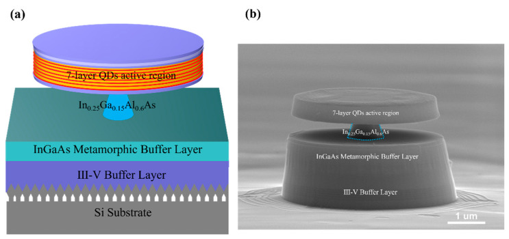
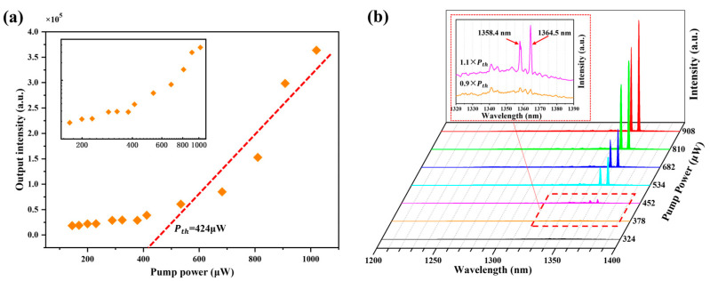
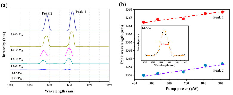
The direct growth of III-V quantum dot (QD) lasers on silicon substrate has been rapidly developing over the past decade and has been recognized as a promising method for achieving on-chip light sources in photonic integrated circuits (PICs). Up to date, O- and C/L-bands InAs QD lasers on Si have been extensively investigated, but as an extended telecommunication wavelength, the E-band QD lasers directly grown on Si substrates are not available yet. Here, we demonstrate the first E-band (1365 nm) InAs QD micro-disk lasers epitaxially grown on Si (001) substrates by using a III-V/IV hybrid dual-chamber molecular beam epitaxy (MBE) system. The micro-disk laser device on Si was characterized with an optical threshold power of 0.424 mW and quality factor (Q) of 1727.2 at 200 K. The results presented here indicate a path to on-chip silicon photonic telecom-transmitters.
Keywords: E-band quantum dots; III-V on silicon; micro-disk lasers; molecular beam epitaxy; photonic integrated circuits.
Conflict of interest statement
The authors declare no conflicts of interest.
Figures
Similar articles
-
1310 nm InAs quantum-dot microdisk lasers on SOI by hybrid epitaxy.Opt Express. 2019 Jul 8;27(14):19348-19358. doi: 10.1364/OE.27.019348. Opt Express. 2019. PMID: 31503695
-
Reduced Dislocation of GaAs Layer Grown on Ge-Buffered Si (001) Substrate Using Dislocation Filter Layers for an O-Band InAs/GaAs Quantum Dot Narrow-Ridge Laser.Micromachines (Basel). 2022 Sep 22;13(10):1579. doi: 10.3390/mi13101579. Micromachines (Basel). 2022. PMID: 36295932 Free PMC article.
-
InAs/GaAs quantum dot laser epitaxially grown on on-axis (001) GaAsOI substrate.Opt Express. 2021 Nov 8;29(23):38465-38476. doi: 10.1364/OE.438678. Opt Express. 2021. PMID: 34808899
-
Mid-infrared III-V semiconductor lasers epitaxially grown on Si substrates.Light Sci Appl. 2022 Jun 1;11(1):165. doi: 10.1038/s41377-022-00850-4. Light Sci Appl. 2022. PMID: 35650192 Free PMC article. Review.
-
Site-controlled growth of In(Ga)As/GaAs quantum dots on patterned substrate.Nanotechnology. 2024 Nov 11;36(5). doi: 10.1088/1361-6528/ad8d61. Nanotechnology. 2024. PMID: 39481133 Review.
Cited by
-
Broad Range Tuning of InAs Quantum Dot Emission for Nanophotonic Devices in the Telecommunication Bands.ACS Appl Nano Mater. 2024 Nov 20;7(23):26854-26862. doi: 10.1021/acsanm.4c04810. eCollection 2024 Dec 13. ACS Appl Nano Mater. 2024. PMID: 39697530 Free PMC article.
References
-
- Asghari M., Krishnamoorthy A.V. Silicon photonics: Energy-efficient communication. Nat. Photonics. 2011;5:268–270. doi: 10.1038/nphoton.2011.68. - DOI
-
- Hu Y., Liang D., Beausoleil R.G. An advanced III-V-on-silicon photonic integration platform. Opto-Electron. Adv. 2021;4:200094. doi: 10.29026/oea.2021.200094. - DOI
-
- Chen S., Li W., Wu J., Jiang Q., Tang M., Shutts S., Elliott S.N., Sobiesierski A.D., Seeds A.J., Ross I.M. Electrically pumped continuous-wave III-V quantum dot lasers on silicon. Nat. Photonics. 2016;10:307–311. doi: 10.1038/nphoton.2016.21. - DOI
Grants and funding
- 62225407, 61975230, 62005308, 12274449, 12304100/National Natural Science Foundation of China
- No. XMYS2023002/Songshan Lake Materials Laboratory
- Y2022005/Youth Innovation Promotion Association
- 2021YFB2800403/National Key Research and Development Program of China
- No. 2021ZD0302300/Innovation Program for Quantum Science and Technology
LinkOut - more resources
Full Text Sources
Miscellaneous
