. 2024 Apr 29;15(1):3622.
doi: 10.1038/s41467-024-47974-2.

Integrated 2D multi-fin field-effect transistors

Affiliations

Integrated 2D multi-fin field-effect transistors

Mengshi Yu et al. Nat Commun. .

Abstract

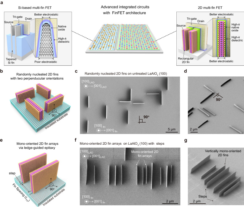
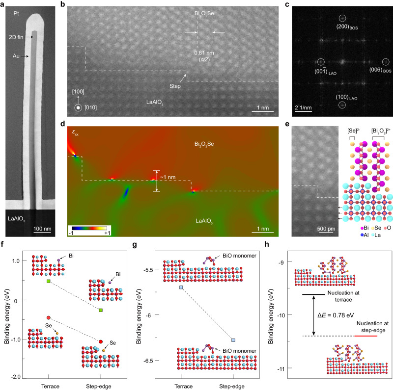
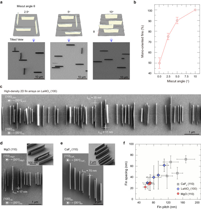
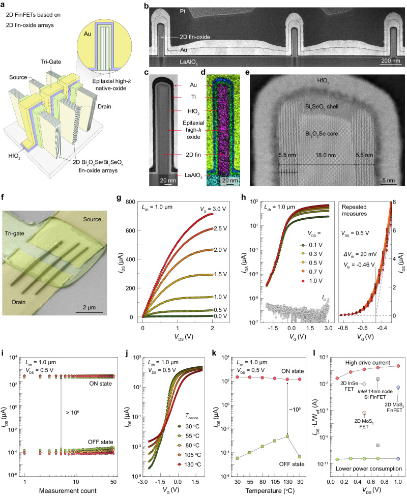
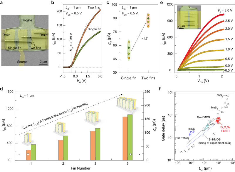
Vertical semiconducting fins integrated with high-κ oxide dielectrics have been at the centre of the key device architecture that has promoted advanced transistor scaling during the last decades. Single-fin channels based on two-dimensional (2D) semiconductors are expected to offer unique advantages in achieving sub-1 nm fin-width and atomically flat interfaces, resulting in superior performance and potentially high-density integration. However, multi-fin structures integrated with high-κ dielectrics are commonly required to achieve higher electrical performance and integration density. Here we report a ledge-guided epitaxy strategy for growing high-density, mono-oriented 2D Bi2O2Se fin arrays that can be used to fabricate integrated 2D multi-fin field-effect transistors. Aligned substrate steps enabled precise control of both nucleation sites and orientation of 2D fin arrays. Multi-channel 2D fin field-effect transistors based on epitaxially integrated 2D Bi2O2Se/Bi2SeO5 fin-oxide heterostructures were fabricated, exhibiting an on/off current ratio greater than 106, high on-state current, low off-state current, and high durability. 2D multi-fin channel arrays integrated with high-κ oxide dielectrics offer a strategy to improve the device performance and integration density in ultrascaled 2D electronics.


Conflict of interest statement

The authors declare no competing interests.

Figures

Fig. 1
Fig. 1. Ledge-guided epitaxy of mono-oriented vertical 2D fin arrays for 2D multi-fin field-effect transistors (FETs).
a Schematic illustration for 2D multi-fin FETs potentially applied in advanced integrated circuits. b–d Schematic (b) and corresponding scanning electron microscopy (SEM) images of 2D Bi2O2Se fins with two perpendicular orientations on pristine LaAlO3 (100) surface, including top view (c) and tilted view (d). e–g Schematic (e) and corresponding SEM images of ledge-guided epitaxial mono-oriented 2D Bi2O2Se fins on pre-treated LaAlO3 (100) surface, including top view (f) and tilted view (g).
Fig. 2
Fig. 2. Structure characterization and nucleation mechanism of vertical 2D fin grown by ledge-guided epitaxy.
a Cross-sectional low-magnification transmission electron microscopy (TEM) image of a vertical Bi2O2Se fin grown by ledge-guided epitaxy. b Cross-sectional high-angle annular dark-field scanning transmission electron microscopy (HAADF-STEM) image showing clear steps on the surface of the substrate, where the fin nucleated. The dashed line means Bi2O2Se/LaAlO3 interface. c Fast Fourier Transform (FFT) diffraction spots of (b). d Strain mapping (ɛxx) estimated from a filtered version of the panel (b). e High-magnification HAADF-STEM image with atomic resolution and corresponding schematic of Bi2O2Se/LaAlO3 interface. The dashed line represents actual interface. f, g The binding energies and optimized structures of Bi/Se atoms (f) and Bi-O monomers (g) adsorbed at the step edge and the terrace of the LaAlO3 substrate, respectively. h The binding energies and optimized structures of a 2D Bi2O2Se nucleus at the step edge and terrace, demonstrate that nucleation at the step edge is energetically favorable. ΔE is the energy difference between two nucleation sites.
Fig. 3
Fig. 3. Guided-growth of mono-oriented high-density 2D fin arrays for 2D multi-fin FETs with the assistance of steps.
a Schematic and SEM images showing the effect of the step density on the orientation of 2D Bi2O2Se fin arrays. b Statistic for mono-oriented fin percentage of 2D Bi2O2Se fin arrays growth with miscut angle of the epitaxial substrate. Error bars indicate standard deviations of mono-oriented fin percentage for different miscut angle. c–e SEM images of high-density 2D Bi2O2Se fin arrays grown by ledge-guided epitaxy on LaAlO3 (100) surface (c), MgO (110) surface (d) and CaF2 (110) surface (e). Insets: corresponding tilted-view high-magnification SEM images. LFS represents fin spacing. f Statistical minimum fin pitch and fin spacing of different vertical 2D Bi2O2Se fin arrays grown by ledge-guided epitaxy on various substrates. Error bars indicate standard deviations of minimum fin spacing and fin pitch for different 2D fin arrays.
Fig. 4
Fig. 4. Electrical performance of 2D multi-fin FinFETs based on aligned 2D Bi2O2Se-Bi2SeO5 fin-oxide arrays.
a Schematic diagram of 2D Bi2O2Se/Bi2SeO5/HfO2 FinFET with three fins. b Cross-sectional STEM image of fin arrays. c–e Low-magnification STEM image (c), Energy-dispersive X-ray spectroscopy (EDS) image (d), and high-magnification STEM image (e) of Bi2O2Se/Bi2SeO5 fin-oxide heterostructures covered with HfO2 dielectric layer. f Tilted SEM image of a 3-fin FinFET. g Typical output curves of the 2D multi-fin FET in (f). IDS is the source-drain current. VDS is the source-drain voltage and VG is the gate voltage. Lch represents the channel length of the devices. h Transfer curves of the 2D multi-fin FET in (f) and the repeated transfer curve measurement results for 50 cycles of the 2D multi-fin FET. IG is the gate leakage current, Vth is the threshold voltage and ΔVth means the shift of threshold voltage. The intersection of the two dashed lines is the threshold voltage of the device, represented by a solid line. i Statistical on-state current (ION) and off-state current (IOFF) measured over 50 cycles for different multiple-channel 2D FinFETs. j, k Transfer curves (j) and statistical ION and IOFF (k) of the 2D multi-fin FET in (f) operated under different temperatures. l Comparison of normalized current of the fabricated 2D multi-fin FETs with 2D MoS2 FET, 2D InSe FET, 2D MoS2 FinFETs and Intel’s 14 nm-node Si FinFETs under low gate-voltage modulation. L is the channel length and Weff is the effective width of device.
Fig. 5
Fig. 5. Comparison of the electrical performances of 2D FinFETs with different number of fins.
a Top SEM image of FinFETs with single fin and two fins, respectively, which share one fin. b Transfer curves of 2D FinFETs with single fin and two fins. c Comparison of the transconductance of 2D FinFETs with single fin and two fins. The different data symbols were obtained from different devices. d Comparison of on-state current and transconductance of 2D FinFETs with different number of fins, demonstrating that multiple-channel FinFETs possess higher electrical performance. e Typical output curves of the 2D FinFETs with five fins. f Benchmarking of the gate delay of 2D multi-fin FETs versus the channel length (Lch) with Si MOS, Ge MOS, MoS2 FET and WS2 FET (Part of data of MoS2 and WS2 are calculated from ref. ,). IRDS 2017–2033 targets for high-performance (HP) transistors are also plotted.

References

    1. Lundstrom MS, Alam MA. Moore’s law: the journey ahead. Science. 2022;378:722–723. doi: 10.1126/science.ade2191. - DOI - PubMed
    1. Liu C, et al. Two-dimensional materials for next-generation computing technologies. Nat. Nanotechnol. 2020;15:545–557. doi: 10.1038/s41565-020-0724-3. - DOI - PubMed
    1. Hu, C. 3D FinFET and other sub-22 nm transistors. In Proc. 19th IEEE International Symposium on the Physical and Failure Analysis of Integrated Circuits 1–5 (2012).
    1. International Roadmap For Devices And Systems 2022 Edition. https://irds.ieee.org/ (2022).
    1. Liu Y, et al. Promises and prospects of two-dimensional transistors. Nature. 2021;591:43–53. doi: 10.1038/s41586-021-03339-z. - DOI - PubMed