. 2024 Jul;11(26):e2400011.
doi: 10.1002/advs.202400011. Epub 2024 May 2.

Erasable and Field Programmable DNA Circuits Based on Configurable Logic Blocks

Affiliations

Erasable and Field Programmable DNA Circuits Based on Configurable Logic Blocks

Yizhou Liu et al. Adv Sci (Weinh). 2024 Jul.

Abstract

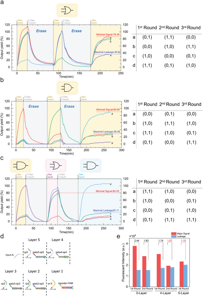
DNA is commonly employed as a substrate for the building of artificial logic networks due to its excellent biocompatibility and programmability. Till now, DNA logic circuits are rapidly evolving to accomplish advanced operations. Nonetheless, nowadays, most DNA circuits remain to be disposable and lack of field programmability and thereby limits their practicability. Herein, inspired by the Configurable Logic Block (CLB), the CLB-based erasable field-programmable DNA circuit that uses clip strands as its operation-controlling signals is presented. It enables users to realize diverse functions with limited hardware. CLB-based basic logic gates (OR and AND) are first constructed and demonstrated their erasability and field programmability. Furthermore, by adding the appropriate operation-controlling strands, multiple rounds of programming are achieved among five different logic operations on a two-layer circuit. Subsequently, a circuit is successfully built to implement two fundamental binary calculators: half-adder and half-subtractor, proving that the design can imitate silicon-based binary circuits. Finally, a comprehensive CLB-based circuit is built that enables multiple rounds of switch among seven different logic operations including half-adding and half-subtracting. Overall, the CLB-based erasable field-programmable circuit immensely enhances their practicability. It is believed that design can be widely used in DNA logic networks due to its efficiency and convenience.

Keywords: DNA logic circuits; DNA nanotechnology; clip‐mediated strand displacement reaction; configurable logic block; field programming.


Conflict of interest statement

The authors declare no conflict of interest.

Figures

Figure 1
Figure 1
a) Schematic illustration of the Configurable Logic Block (CLB) in digital circuits. b) Schematic illustration of CLB‐based erasable field‐programmable DNA circuits. The clip strands were used as the operation‐controlling signals so that adding different clips could result in different logic operations. Also, the clip strands enabled the circuit to be erased by adding their complementary strands. c) Schematic illustration of CLB‐based erasable field‐programmable OR and AND gate. Adding different clips (operation‐controlling strands) would lead to corresponding logic operations, and the initial state could be restored by adding C‐clips and C‐inputs. X* and X were designed to be complementary, where “X” stands for different domain names. d) Experimental verification of OR gate. e) Experimental verification of AND gate. Reaction setup: 100 nm (5 pmol) FAM:BHQ,120 nm (6 pmol) clips, 240 nm inputs (12 pmol) were added sequentially to form a system with final volume of 50 µL. All experiments depicted in the figure were replicated at least twice, with consistent trends observed.
Figure 2
Figure 2
Experimental verification of the field programmability of the CLB‐based OR and AND gate. a) The fluorescent curves of the OR gate reusing for 3 times. b) The fluorescent curves of the AND gate reusing for 3 times. c) The fluorescent curves of the logic gate switched in the order of AND‐OR‐AND. Reactions setup: 100 nm (5 pmol) FAM:BHQ, 120 nm (6 pmol) operation‐controlling strands, 240 nm (12 pmol) inputs were added sequentially to form a system with a final volume of 50 µL for the first‐round using; 120 nm (6 pmol) C‐clips, 240 nm (12 pmol) C‐inputs for the first‐round erasing. The concentration of inputs/clips and C‐input/clips would increase 10 nm each round. d) The schematic illustration of the multilayer Translator system. e) Experiment Results of first (and second) round running for multilayer translator circuits. Reaction setup: 100 nm (5 pmol) FAM:BHQ, 120 nm (6 pmol) or‐fi was added. Afterward, the gate:output and clip, or input, of the upper layer circuit were added, with a concentration twice that of the lower layer. The final volume for the first‐time use was 50 µL. For erasability, the complementary strands (c‐clips and c‐inputs) were added with equal quantity to the clip and input strands in the forward reaction. For each round's reusing, the clip and input strands were added with a concentration increase of 10 nm compared to the previous round. All experiments depicted in the figure were replicated at least twice, with consistent trends observed.
Figure 3
Figure 3
a,b) Schematic illustration and logic operation table of the CLB‐based “X‐AND” gate. There are two positions for users to add operation‐controlling strands to realize five different logic operations. c) Digital circuit diagram of “A AND B AND C” and the schematic illustration of its corresponding CLB‐based DNA circuit. The pattern inside the blue box shows the location of the “incumbent toehold”. d,e) The fluorescent curves of “(A OR D) AND (B OR C)”and “A AND B AND C”. Reactions setup: 100 nm (5 pmol) FAM:BHQ, 240 nm (12 pmol) gate2:output2 and gate1:output1, 120 nm (6 pmol) and1, 240 nm (12 pmol) operation controlling strands and inputs were added sequentially to form a system with final volume of 50 µL. f) The fluorescent curves of “X‐AND” gate switched in the order of (A AND D AND B AND C)‐(A AND B AND C)‐(A AND B). g) The heat map reflects the output yield of “A AND B AND C AND D” in a 3‐round reusing. h) The comparison of signal‐to‐noise ratio between logic‐switching and reusing “A AND B AND C AND D”. Reactions setup: 100 nm (5 pmol) FAM:BHQ, 240 nm (12 pmol) gate2:output2 and gate1:output1, 120 nm (6 pmol) and1, 240 nm (12 pmol) operation controlling strands and inputs to form a system with a final volume of 50 µL for the first‐time using. 120 nm (6 pmol) c‐and1, 240 nm (12 pmol) c‐clips/inputs were added for the first time erasing. The concentration of inputs/clips and C‐input/clips would increase 10 nm each round. All experiments depicted in the figure were replicated at least twice, with consistent trends observed.
Figure 4
Figure 4
a) Schematic illustration of integrating a half‐adder and a half subtractor into one dual‐rail comprehensive circuit. Inside the dashed box illustrates the digital circuit diagram of half‐adder/subtractor and their corresponding CLB‐based DNA circuit. b) Logic operation table of the integrated comprehensive circuit. * Input‐1, 2, 3, or 4 in different logic operations does not stand for the same strand.** The corresponding logic operations were dual‐rail. The output yield of half‐adder c), half‐subtractor d), “1 OR 2 OR 3 OR 4” e), “(1 AND 2) OR 3 OR 4” f), XOR g), “1 AND 2” h), “1 OR 2” i). Note that the matrix was arranged in the order of Reactions setup: 100 nm (5 pmol) FAM:BHQ and HEX:HBHQ, 240 nm (12 pmol) gate1:output, gate2:output and gate3:ouputA*, 120 nm (6 pmol) or‐fi, 240 nm (12 pmol) operation‐controlling strands and 480‐nm input strands were added sequentially to form a system with final volume of 50 µL. All experiments depicted in the figure were replicated at least twice, with consistent trends observed.
Figure 5
Figure 5
a) Fluorescent curves of XOR gate reusing 3 times. b) Fluorescent curves of the comprehensive logic gate switched in the order of XOR‐(1 OR 2 OR 3 OR 4). c) Fluorescent curves of the comprehensive logic gate switched in the order of XOR‐half adder‐XOR. d) Fluorescent curves of the comprehensive logic gate switched in the order of XOR‐half subtractor‐XOR. Reactions setup: 100 nm (5 pmol) FAM:BHQ and HEX:HBHQ, 240 nm (12 pmol) gate1:output, gate2:output and gate3:ouputA*, 120 nm (6 pmol) or‐fi, 240 nm (12 pmol) operation‐controlling strands and 480‐nm input strands were added to form a system with final volume of 50 µL for the first‐time using; 120 nm (6 pmol) c‐or‐fi, 240 nm (12 pmol) C‐clips and 480‐nm C‐inputs were added for the first‐time restoring. The concentration of inputs/clips and C‐input/clips would increase 10 nm each round. All experiments depicted in the figure were replicated at least twice, with consistent trends observed.

Similar articles

References

    1. Fu T., Lyu Y., Liu H., Peng R., Zhang X., Ye M., Tan W., Trends Biochem. Sci. 2018, 43, 547. - PMC - PubMed
    1. Song X., Reif J., ACS Nano 2019, 13, 6256. - PubMed
    1. Zhao S., Yu L., Yang S., Tang X., Chang K., Chen M., Nanoscale Horiz. 2021, 6, 298. - PubMed
    1. Qian L., Winfree E., Bruck J., Nature 2011, 475, 368. - PubMed
    1. Zhang C., Ge L., Zhuang Y., Shen Z., Zhong Z., Zhang Z., You X., Sci. China Inf. Sci. 2019, 62, 61301.

LinkOut - more resources