. 2024 May 29;16(21):27523-27531.
doi: 10.1021/acsami.4c02525. Epub 2024 May 15.

Nonvolatile Modulation of Bi2O2Se/Pb(Zr,Ti)O3 Heteroepitaxy

Affiliations

Nonvolatile Modulation of Bi2O2Se/Pb(Zr,Ti)O3 Heteroepitaxy

Yong-Jyun Wang et al. ACS Appl Mater Interfaces. .

Abstract

The pursuit of high-performance electronic devices has driven the research focus toward 2D semiconductors with high electron mobility and suitable band gaps. Previous studies have demonstrated that quasi-2D Bi2O2Se (BOSe) has remarkable physical properties and is a promising candidate for further exploration. Building upon this foundation, the present work introduces a novel concept for achieving nonvolatile and reversible control of BOSe's electronic properties. The approach involves the epitaxial integration of a ferroelectric PbZr0.2Ti0.8O3 (PZT) layer to modify BOSe's band alignment. Within the BOSe/PZT heteroepitaxy, through two opposite ferroelectric polarization states of the PZT layer, we can tune the Fermi level in the BOSe layer. Consequently, this controlled modulation of the electronic structure provides a pathway to manipulate the electrical properties of the BOSe layer and the corresponding devices.

Keywords: 2D semiconductor; Bi2O2Se; electronic potential; ferroelectric; nonvolatile modulation.


Conflict of interest statement

The authors declare no competing financial interest.

Figures
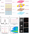
Figure 1
Figure 1
(a) Schematic diagram of the BOSe/PZT/SRO/STO heterostructure. (b) Normal scan of the (00L) series of STO with BOSe (006), PZT (002), and SRO (002) of the heterostructure. (c) Phi scans of STO(202), SRO(202), PZT(202), and BOSe(101). (d) Rocking curves of the as-grown SRO, PZT, and BOSe thin films. (e) Reciprocal space mappings of SRO, PZT, and BOSe on the STO substrate. (f) The cross-sectional STEM-HAADF images of the BOSe/PZT/SRO interfaces and their FFT patterns.
Figure 2
Figure 2
(a) PFM out-of-plane phase image after the poling process. (b) KPFM surface potential detected directly after the PFM measurement. The band structure of the BOSe/PZT heterointerface probed by XPS measurements. (c, d) BE alteration of Bi and Pb ions and (e, f) schematic diagrams illustrating the energy band alignment at the BOSe/PZT heterointerface under the Pdown and Pup states.
Figure 3
Figure 3
(a) Schematic diagram of the scanning tunneling microscopy with the comparison of the Pup and Pdown states. (b, c) Topography and DOS mapping images from the cross-sectional direction at 77 K. The spatial spectroscopic measurements on (d, e) Nb:STO/SRO and PZT interfaces. (f) BOSe of BOSe/PZT/SRO/Nb:STO system under the Pup and Pdown states.
Figure 4
Figure 4
Electron characteristics of the synthesized FeFET system. (a) Schematic diagram of the Hall measurement. (b, c) Results of the Hall measurements and resistivity-temperature curves for BOSe under nonpoled, Pup, and Pdown states. (d) Schematic diagram of the PV and CV loop measurements on the MFS capacitor. (e, f) Results of the PV and CV loop measurements and increasing gate voltage from 1 to 8 V at an AC frequency of 10 kHz. (g) Schematic diagram of the fabricated bottom-gate FeFET device. (h, i) The transfer characteristics (IDVG and IDVD) of the FeFET.

References

    1. Sun Y.; Zhang J.; Ye S.; Song J.; Qu J. Progress Report on Property, Preparation, and Application of Bi2O2Se. Adv. Funct. Mater. 2020, 30, 200448010.1002/adfm.202004480. - DOI
    1. Li T.; Peng H. An Emerging Material Platform for the Next-Generation Electronic Industry. Acc. Mater. Res. 2021, 2, 842–853. 10.1021/accountsmr.1c00130. - DOI
    1. Fu Q.; Zhu C.; Zhao X.; Wang X.; Chaturvedi A.; Zhu C.; Wang X.; Zeng Q.; Zhou J.; Liu F.; Tay B. K.; Zhang H.; Pennycook S. J.; Liu Z. Ultrasensitive 2D Bi2O2Se Phototransistors on Silicon Substrates. Adv. Mater. 2019, 31, 180494510.1002/adma.201804945. - DOI - PubMed
    1. Chen W.; Zhang R.; Zheng R.; Liu B. Out-of-Plane Resistance Switching of 2D Bi2O2Se at the Nanoscale. Adv. Funct. Mater. 2021, 31, 210579510.1002/adfm.202105795. - DOI
    1. Zhang J.; Li H. Bi2O2Se:Bi2O5Se High-K Stack as a 2D Analog of Si:SiO2: A First-Principles Study. Phys. Status Solidi (RRL) 2021, 15, 200046510.1002/pssr.202000465. - DOI