. 2024 Apr 27;7(9):4004-4015.
doi: 10.1021/acsaem.4c00303. eCollection 2024 May 13.

Zirconium Oxynitride Thin Films for Photoelectrochemical Water Splitting

Affiliations

Zirconium Oxynitride Thin Films for Photoelectrochemical Water Splitting

Verena Streibel et al. ACS Appl Energy Mater. .

Abstract

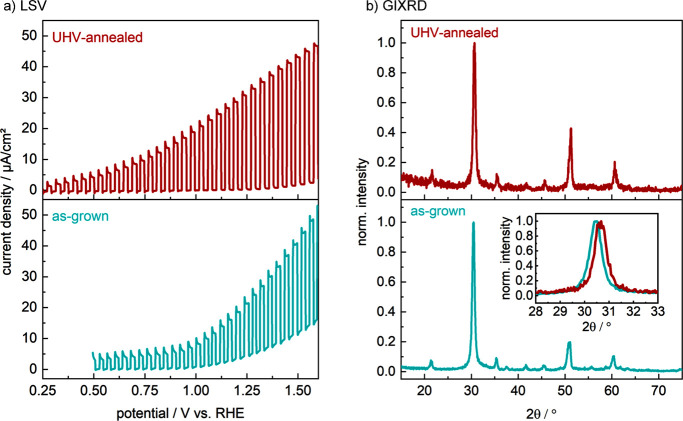
Transition metal oxynitrides are a promising class of functional materials for photoelectrochemical (PEC) applications. Although these compounds are most commonly synthesized via ammonolysis of oxide precursors, such synthetic routes often lead to poorly controlled oxygen-to-nitrogen anion ratios, and the harsh nitridation conditions are incompatible with many substrates, including transparent conductive oxides. Here, we report direct reactive sputter deposition of a family of zirconium oxynitride thin films and the comprehensive characterization of their tunable structural, optical, and functional PEC properties. Systematic increases of the oxygen content in the reactive sputter gas mixture enable access to different crystalline structures within the zirconium oxynitride family. Increasing oxygen contents lead to a transition from metallic to semiconducting to insulating phases. In particular, crystalline Zr2ON2-like films have band gaps in the UV-visible range and are n-type semiconductors. These properties, together with a valence band maximum position located favorably relative to the water oxidation potential, make them viable photoanode candidates. Using chopped linear sweep voltammetry, we indeed confirm that our Zr2ON2 films are PEC-active for the oxygen evolution reaction in alkaline electrolytes. We further show that high-vacuum annealing boosts their PEC performance characteristics. Although the observed photocurrents are low compared to state-of-the-art photoanodes, these dense and planar thin films can offer a valuable platform for studying oxynitride photoelectrodes, as well as for future nanostructuring, band gap engineering, and defect engineering efforts.


Conflict of interest statement

The authors declare no competing financial interest.

Figures

Figure 1
Figure 1
(a) Structural motifs of two neighboring Zr atoms within ZrN, cubic Zr3N4, bixbyite-type Zr2ON2, and fluorite-type ZrO2. Only portions of the unit cell are shown for better visualization of the Zr–O–N coordination. Zr atoms are shown in gray, oxygen in red, and nitrogen in blue, generated with VESTA. (b) Grazing incidence X-ray diffraction (GIXRD) patterns of sputter-deposited ZrxOyNz films, along with reference patterns of ZrN (dark violet), Zr3N4 (dark blue), bixbyite-type Zr2ON2 (turquoise), and fluorite-type ZrO2 (green). Films were deposited with variable amounts of oxygen (as indicated in the legend on the left) and a constant flow of 20 sccm N2 and 10 sccm Ar. At approximately 52°, a reflection of the crystalline Si(100) substrate is visible; all other reflections can be attributed to the different ZrxOyNz crystalline phases. (c) UV–vis transmission spectra corresponding to the films shown in panel b.
Figure 2
Figure 2
Elemental composition of the ZrxOyNz films based on (a) energy-dispersive X-ray spectroscopy (EDX) and (b) X-ray photoelectron spectroscopy (XPS).
Figure 3
Figure 3
XPS spectra of the (a) O 1s, (b) N 1s, and (c) Zr 3d core-level regions of a selection of the deposited ZrxOyNz films (the oxygen content in the reactive sputter gas mixture is indicated in panel a). Identified species are marked with vertical lines. In the O 1s spectrum, it is not possible to deconvolute the contribution of ZrO2 and ZrxOyNz.
Figure 4
Figure 4
Ultraviolet photoelectron spectroscopy (UPS) measurement of a representative Zr2ON2 thin film using the He I emission line. The secondary electron cutoff (SECO) and the valence band maximum (VBM) positions are indicated by dotted, intercepting lines, along with the respective values. The work function, Φ, is calculated by the difference of the He I emission line energy and the SECO. The inset shows the energy level diagram of the system, where Evac marks the vacuum level, ECBM is the conduction band minimum, EF the Fermi level, EVBM is the valence band maximum, and, for comparison, H2O/H2 and O2/OH represent the water reduction and oxidation potentials, respectively.
Figure 5
Figure 5
Linear sweep voltammograms (LSVs) of different ZrxOyNz films on Si substrates deposited with varying oxygen contents in the reactive gas mixture as indicated in the figure (as in Figure 1). The LSVs were recorded in 1 M NaOH under chopped front-side illumination (AM 1.5G, 100 mW/cm2). The insets for the 0.08 and 0.12 sccm O2 samples show the zoomed-out versions of the LSVs to demonstrate the film self-oxidation peaks at 1.3 and 1.2 V vs RHE, respectively.
Figure 6
Figure 6
Optical and compositional analysis of a representative Zr2ON2 thin film. (a) Variable angle spectroscopic ellipsometry data (for clarity, presented for a single angle of 45°), along with the fit obtained using a general oscillator (GenOsc) model. (b) Corresponding transmission data and predicted transmission spectrum based on the GenOsc model derived from the ellipsometry data in panel a. The inset in panel b shows a model of the sample. The best fit was obtained for a graded layer of ZrxOyNz on a SiO2 substrate. (c) Representative refractive index, n, and extinction coefficient, k, obtained for the top and bottom layers of the GenOsc model in panel a. Reduced n and k values are indicative of a higher oxygen content. (d) Elastic recoil detection analysis (ERDA) measurements of the same sample. Note that the depth scale in nm is only an approximation based on the calculated film density.
Figure 7
Figure 7
(a) Linear sweep voltammograms (LSVs) and (b) grazing incidence X-ray diffraction (GIXRD) patterns of ZrxOyNz films on Si substrates, (bottom) as-deposited and (top) following postsynthetic high-vacuum annealing at 700 °C for 40 min. The LSVs were recorded in 1 M NaOH under chopped front-side illumination (AM 1.5G, 100 mW/cm2) at a sweep rate of 20 mV/s. High-vacuum annealing results in increased photocurrent density, decreased dark current density, and a beneficial cathodic shift of the open circuit potential (from which the LSVs were initiated). The inset in panel b shows a zoomed-in comparison of the most intense reflection of the as-grown and UHV-annealed samples at 30.5°. Annealing does not significantly affect the fwhm of the diffraction patterns but leads to a shift of the reflection angle by 0.2° toward higher angles.

References

    1. Brown J. J.; Ke Z.; Ma T.; Page A. J. Defect Engineering for Photocatalysis: From Ternary to Perovskite Oxynitrides. ChemNanoMat 2020, 6 (5), 708–719. 10.1002/cnma.201900703. - DOI
    1. Ahmed M.; Xinxin G. A review of metal oxynitrides for photocatalysis. Inorg. Chem. Front. 2016, 3 (5), 578–590. 10.1039/C5QI00202H. - DOI
    1. Castelli I. E.; García-Lastra J. M.; Hüser F.; Thygesen K. S.; Jacobsen K. W. Stability and bandgaps of layered perovskites for one- and two-photon water splitting. New J. Phys. 2013, 15 (10), 105026.10.1088/1367-2630/15/10/105026. - DOI
    1. Sun W.; Bartel C. J.; Arca E.; Bauers S. R.; Matthews B.; Orvañanos B.; Chen B. R.; Toney M. F.; Schelhas L. T.; Tumas W.; Tate J.; Zakutayev A.; Lany S.; Holder A. M.; Ceder G. A map of the inorganic ternary metal nitrides. Nat. Mater. 2019, 18 (7), 732–739. 10.1038/s41563-019-0396-2. - DOI - PubMed
    1. Fuertes A. Synthetic approaches in oxynitride chemistry. Prog. Solid State Chem. 2018, 51, 63–70. 10.1016/j.progsolidstchem.2017.11.001. - DOI