Review
. 2024 Jul;11(27):e2305611.
doi: 10.1002/advs.202305611. Epub 2024 May 17.

Advanced Neuromorphic Applications Enabled by Synaptic Ion-Gating Vertical Transistors

Affiliations
Review

Advanced Neuromorphic Applications Enabled by Synaptic Ion-Gating Vertical Transistors

Leandro Merces et al. Adv Sci (Weinh). 2024 Jul.

Abstract

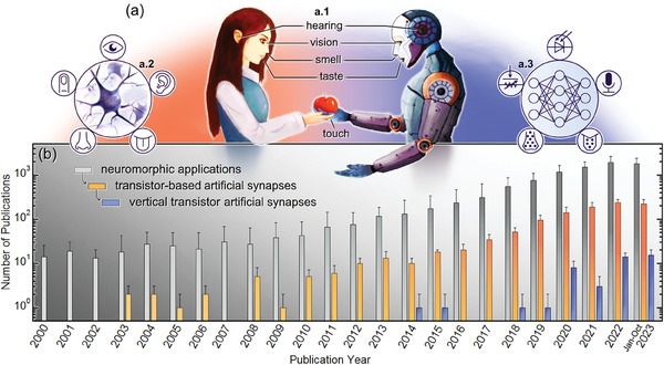
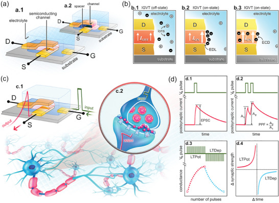
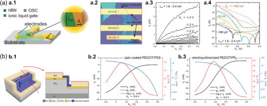
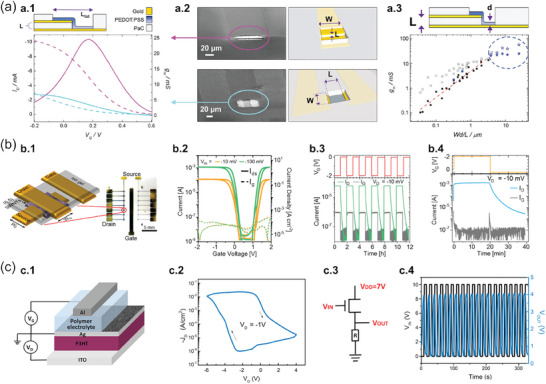
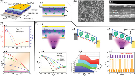
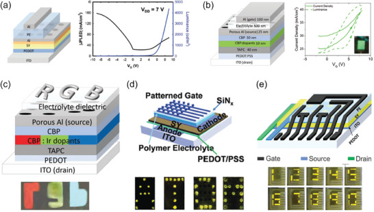
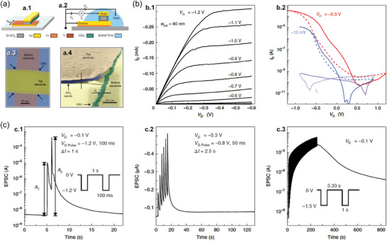
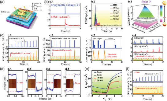
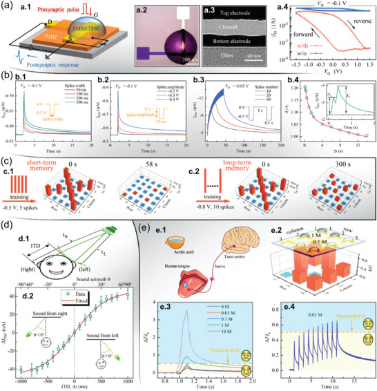
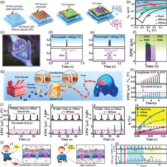
Bioinspired synaptic devices have shown great potential in artificial intelligence and neuromorphic electronics. Low energy consumption, multi-modal sensing and recording, and multifunctional integration are critical aspects limiting their applications. Recently, a new synaptic device architecture, the ion-gating vertical transistor (IGVT), has been successfully realized and timely applied to perform brain-like perception, such as artificial vision, touch, taste, and hearing. In this short time, IGVTs have already achieved faster data processing speeds and more promising memory capabilities than many conventional neuromorphic devices, even while operating at lower voltages and consuming less power. This work focuses on the cutting-edge progress of IGVT technology, from outstanding fabrication strategies to the design and realization of low-voltage multi-sensing IGVTs for artificial-synapse applications. The fundamental concepts of artificial synaptic IGVTs, such as signal processing, transduction, plasticity, and multi-stimulus perception are discussed comprehensively. The contribution draws special attention to the development and optimization of multi-modal flexible sensor technologies and presents a roadmap for future high-end theoretical and experimental advancements in neuromorphic research that are mostly achievable by the synaptic IGVTs.

Keywords: artificial synapses; brain‐inspired; electrochemical; field effects; human‐machine interfacing; multi‐modal; sensors.


Conflict of interest statement

The authors declare no conflict of interest.

Figures

Figure 1
Figure 1
Human‐brain‐inspired multisensory functions and neuromorphic research. a) Schematic illustrations of a.1) the five primary sensory systems in the human body, a.2) multisensory functions processed by the human brain, and a.3) their emulation by artificial neural networks. Adapted with permission.[ 12 ] Copyright 2021, Tan et al. Published by Springer Nature. b) The increasing number of publications regarding neuromorphic applications (viz. logarithmic scale) over the past years to October 2023. Data collected from Web of Science on November 2023. Examination fluctuations (upper error bars) arise from possible keyword combinations, article categorization, and search refinement.
Figure 2
Figure 2
IGVT device architecture, working principle, and synaptic functions. a) Schematic illustrations of the IGVT basic structures, in which a.1) the semiconductor film is sandwiched by S and D, or a.2) a spacer layer is employed to set the S‐to‐D separation. b) Illustration of the p‐type IGVT working principle (without loss of generality). b.1) IGVT OFF‐state. b.2) IGVT ON‐state: EDL formation leading to the electric‐field effect and EG‐V(O)FET current amplification. b.3) IGVT ON‐state: ECD leading to the mixed ionic and electronic current amplification across the V(O)ECT channel. c) Artificial synapse concept. c.1) Schematic illustration of an artificial synapse based on the IGVT. c.2) Schematic illustration of a neural network and zoom in the biological synapse. d) Functions of synaptic devices. d.1) EPSC and d.2) PPF induced by single‐ and double‐pulse input stimuli. d.3) LTPot and LTDep triggered by multiple pulses. d.4) STDP in response to LTPot and LTDep.
Figure 3
Figure 3
IGVT devices, materials, and electrical characterization. a) EG‐VOFETs with ultrashort L values. a.1) Illustration of the device architecture. The zoomed‐in image shows that the spacer thickness is the L of the transistor. a.2) Optical microscopy image of EG‐VOFETs with three top terminals sharing the same bottom electrode and the same hBN layer. a.3) Output curves acquired at a VD sweep rate of 10 mV s−1 and a.4) transfer curves measured at a VG sweep rate of 20 mV s−1. In both electrical characteristics, the solid lines are related to the forward sweep direction, and the dashed lines in a.4) correspond to the backward one. Adapted with permission.[ 37 ] Copyright 2021, American Chemical Society. b) Scalable and reliable method for downsizing L of VOECTs. b.1) Sketch of the proposed device composed of a spin‐coated PEDOT:PSS layer together with its cross‐section view. Transfer curves of b.2) a 400 nm‐thick spin‐coated PEDOT:PSS VOECT and b.3) a 280 nm‐thick electropolymerized PEDOT:PF6 device. All VOECTs had W = 100 µm and L = 350 nm. Adapted with permission.[ 94 ] Copyright 2023, Brodský et al. Published by American Chemical Society.
Figure 4
Figure 4
High‐performance IGVTs and the IGVT‐based inverter. a) Influence of transistor geometry on its performance. a.1) VOECT architecture with a PaC spacer between S and D. The L is equal to the PaC thickness. The bottom panel shows the transfer curves (dashed lines) acquired at VD = −0.6 V and the transconductance curves (solid lines) for vertical and planar transistors. VOECT responses are shown in magenta, and responses for the planar device are in cyan. a.2) SEM images (left column) and sketches (right column) of the VOECT and planar device. The images illustrate the L and W properties of the transistors according to their geometries. a.3) The upper panel illustrates d of the channel material. The bottom panel exhibits the influence of the W, d, and L properties on g m. Blue stars are g m for VOECTs. The squares correspond to data for planar devices acquired by Donahue et al. (blue squares)[ 66 ] and by Rivnay et al. (black squares).[ 64 ] Full symbols designate the experimentally obtained transconductance, whereas the open ones relate to intrinsic transconductance. Adapted with permission.[ 66 ] Copyright 2017, WILEY‐VCH. b) Vertical transistor geometry for dynamic measurements. b.1) Sketch of the IGVT fabricated with aerosol‐jet‐printed layers of polymer‐sorted (6,5) SWNTs, evaporated Au or printed Ag nanoparticles terminals, and an ionic‐gel electrolyte. The real sample contains 14 transistors and one G as shown in the optical microscopy image. b.2) Transfer curve and b.3) switching behavior for IGVTs without metallic SWNTs and pure ionic liquid electrolyte. In b.3), the device was turned on or off by changing VG from −0.2 V to 0 V, respectively. b.4) Switching behavior for IGVT composed of aerosol jet printed Ag nanoparticle electrodes and (6,5) SWNTs. VG ranged from 0 V to −2 V, changing after 20 min to 0.5 V. Adapted with permission.[ 55 ] Copyright 2018, American Chemical Society. (https://pubs.acs.org/doi/full/10.1021/acsanm.8b00756. Further permissions related to the material excerpted should be directed to the ACS.) c) Possibility of using IGVTs in simple circuits. c.1) Illustration of the device structure composed of PEDOT‐coated ITO, P3HT as the channel material, a polymer electrolyte, a 30 nm thick Ag porous electrode, and an Al G‐terminal. The P3HT thickness corresponds to L. c.2) Transfer characteristic for the IGVT. c.3) Circuit diagram of the inverter based on IGVT loaded as a resistor. c.4) Dynamic responses of the inverter to rectangular voltage input. Adapted with permission.[ 102 ] Copyright 2018, American Chemical Society.
Figure 5
Figure 5
Vertically stacked complementary circuits based on VOECTs. a) Device fabrication, structure, and morphology. a.1) S‐OSC‐D base structure (left) and assembled VOECT (right‐hand side). a.2) Optical microscopy image of a p‐type VOECT. The electrode overlap region is zoomed in (W = L = 70 µm). a.3) Cross‐section illustration of p‐type VOECT (zoom‐in: false‐color cross‐section SEM image). b) VOECT performance and comparison with the planar counterpart and the literature. b.1) Schematics illustrating the differences in typical planar‐ and vertical device geometry. b.2–4) g m vs. Wd/L, I ON/OFF vs. g m, and I ON/OFF vs. I ON, respectively, for the reported OECTs.[ 18 , 40 , 107 , 108 , 110 , 111 , 112 , 113 , 114 , 115 , 116 , 117 , 118 , 119 , 120 ] c) Complementary inverter based on 2 VOECTs: c.1) illustration of vertical stacking, c.2) top view of 2‐VOECT inverter, and c.3) 10 Hz switching stability of 2‐VOECT inverter. d) VOECT‐based logic circuits: optical images of d.1) NAND‐ and d.2) NOR circuits, d.3) NAND and NOR input/output characteristics, d.4) optical image of the rectifier, and d.5) rectifier input/output characteristics. Adapted with permission.[ 54 ] Copyright 2023, Huang et al. Published by Springer Nature.
Figure 6
Figure 6
VOECT‐based ambipolar inverters and application as a bio‐signal amplifier. a) Device structure: a.1) cross‐sectional view of the cofacial pair of OECTs illustrating materials, dimensions, and contacts; a.2) SEM image of the cross‐section of the cofacial pair of OECTs. Scale bar, 1 µm. b) Planar‐ and vertical‐device electric characteristics. Panels b.1) and b.2) exhibit the planar OECT configurations, whereas b.3) exhibits their output characteristics. Panels b.4) and b.5) exhibit the VOECT configurations, whereas b.6) exhibits their highly modulated output characteristics (compared with planar OECTs). Panel b.7) depicts the transfer characteristics of the planar‐ and VOECTs. c) VOECTs applied as complementary inverter: c.1) illustration of the cross‐section view of cofacial OECTs circuited as a complementary inverter; c.2) microscopic image of the inverter top view; c.3) transfer curves for the inverter; c.4) sinusoidal input with the corresponding amplified output. d) ECG signal amplification acquired with a complementary inverter. d.1) Voltage preamplifier wiring diagram. Medical electrodes are attached to the right and left sides of the body, below the clavicle. They are connected to a direct current offset and the input of the inverter on a digital multimeter. d.2) Signal recorded from the output of the VOECT inverter. d.3) Signal between the medical electrodes acquired with the digital multimeter. Adapted with permission.[ 131 ] Copyright 2021, Rashid et al. Published by AAAS.
Figure 7
Figure 7
VOECTs for low‐amplitude micro‐organ signal processing. a) VOECT geometrical structure. b) Block diagram of the data flow and acquisition process. c) Device‐specific board connecting all VOECTs/electrodes to the CHOSEI board. d) ID vs. VG and g m vs. VG curves of VOECT array covered with HL‐1 cells for the recording of action potentials. e) Extracted mean configuration of HL‐1 action potentials obtained using VOECTs in comparison with electrodes. f) Signal‐to‐noise ratios, action potential amplitudes, and action potential frequency of HL‐1 cells. g,h) Action potential amplitudes and frequencies, and slow potential amplitudes and frequencies at low and high glucose concentrations. Adapted with permission.[ 138 ] Copyright 2022, Abarkan et al. Published by Wiley‐VCH.
Figure 8
Figure 8
Monolithic tandem VOECTs for printed multivalued logic applications. a) Device geometry of dual‐channel VOECT with P3HT‐PEDOT:PSS vertically stacked channels. b) Simulated and measured V OUT vs. V IN, and c) signal gain of a ternary inverter based on a dual‐channel VOECT. d) Logic circuit diagrams and images of the VOECT‐based NMIN gate and the e) VOECT‐based NMAX gate. f) V OUT and V IN as a function of time of NMIN and NMAX gates. Adapted with permission.[ 31 ] Copyright 2023, Wiley‐VCH.
Figure 9
Figure 9
Vertical‐channel organic/inorganic hybrid electrochemical phototransistors. a) Schematic illustrations of a.1) the hybrid optoelectronic device based on the VECT architecture with nanoscale L, and a.2) the VECT electrical circuit. b) SEM images of b.1) the AgNW S, and b.2) the VECT cross‐section. c) Electrical characterization of the VECT: c.1) transfer‐ and transconductance characteristics, and c.2) output characteristics. d) Phototransistor working principle and optoelectronic performance: d.1) illustration of the phototransistor under 365 nm illumination, d.2) schematic mechanism of VECT conduction, d.3) schematic mechanism of the UV light‐induced photocurrent, d.4) transfer curves acquired at dark condition and different UV intensities, d.5) responsiveness for VG under various illumination intensities, and d.6) temporal response to 10 periods of 365 nm illumination with 1000 µW cm−2. Adapted with permission.[ 148 ] Copyright 2021, American Chemical Society.
Figure 10
Figure 10
Light‐emitting EG‐VOFETs. Structures of light‐emitting EG‐VOFETs where the porous S of Al enables contact between the electrolyte and the organic layer comprised of: a) the SY polymer emitter, and b) a mixture of CBP host doped with Ir‐dopant phosphorescent guest. The electrical characteristic curves for the devices are exhibited in the right‐hand panels in (a,b). c) Light‐emitting EG‐VOFET‐based prototype display composed of a light‐emitting material doped with three different‐color components. The three G electrodes were patterned to display in red, green, and blue the initial letters of each color. d) An array consisting of G terminals that can be individually turned on to display letters. e) Light‐emitting EG‐VOFET with seven G electrodes that are controlled at different times to display numbers from 0 to 9. (a,d) Adapted with permission.[ 159 ] Copyright 2016, WILEY‐VCH. (b,c) Adapted with permission.[ 160 ] Copyright 2017, American Chemical Society. e) Adapted with permission.[ 161 ] Copyright 2017, American Chemical Society.
Figure 11
Figure 11
Artificial synaptic behavior in nanoscopic EG‐VOFETs. a) Device structure and microscopy images. a.1) Patterned device base structure (viz. bottom‐ and top electrodes, SiO2 spacer, and OSC). a.2) Schematic circuit for the electrical characterization. The materials are labeled at the bottom, whereas W bel is the bottom‐electrode width. a.3) Polarization microscopy image of the EG‐VOFET without electrolyte G. a.4) False‐color SEM image of the EG‐VOFET. b) EG‐VOFET electrical characteristics: b.1) output‐ and b.2) transfer curves. c) STP and LTP of the EG‐VOFET. c.1) EPSC activated by two −1.2 V‐presynaptic spikes lasting 100 ms each, spaced by one second. c.2) EPSC dynamic response to six G spikes of −0.8 V for 50 ms, spaced by 2.5 s apart. c.3) EPSC activated by 73 spikes of −1.5 V lasting one second and spaced 3.33 s for a device featuring only OSC between S and D. Adapted with permission.[ 69 ] Copyright 2019, Lenz et al. Published by Springer Nature .
Figure 12
Figure 12
Sub‐10 nm organic‐inorganic EG‐VFET for nociceptor emulation. a) Schematics of the EG‐VFET structure and functional components. b) EPSC and pain threshold: b.1) EPSC for a presynaptic pulse of 2 V lasting 10 ms (VD  = 2 V), b.2) EPSCs for different frequencies (2–50 Hz), b.3) spike‐rate dependent plasticity as a function of stimuli number and frequency (threshold plane: 25 µA cm−2). c) EG‐VFET response to electrical pulses: c.1) 10 ms pulse width and 0.4–1.9 V amplitude, c.2) 0.6 V amplitude pulses lasting from 10 to 200 ms, c.3) 2 V amplitude followed by 0.8 V amplitude pulse train with 10 ms‐10 s time interval between the two continuous stimulus trains, and c.4) 1.2–2.0 V amplitude before a set of 0.4 V amplitude pulses. Spikes were spaced by 1 ms. d) Height profiles and AFM images (insets) of the ITO channel edges of d.1) 3 nm, d.2) 8 nm, d.3) 15 nm, and d.4) 24 nm thick samples. e) EG‐VFET transfer curves at VD  = 2 V for different channel thicknesses. f) Pulsed evaluation of 8 nm thick channel EG‐VFET. Adapted with permission.[ 36 ] Copyright 2019, WILEY‐VCH.
Figure 13
Figure 13
VOECT artificial synapse expandable to a crossbar array. a) Optical microscopy image of the ANN. The inset shows the top view of a device. b) Sketch of the three‐terminal synaptic device at each crossing point of the presynaptic and postsynaptic electrodes in the ANN. The inset illustrates the negative ions of the ion‐gel penetrating or moving out from the free volume of the channel when a negative or positive V WC is applied, respectively. c) LTPot/Dep curves for vertical synaptic devices with different P3HT thicknesses under 100/100 potentiation/depression V WC pulses of −3 and +2 V. d) LTPot/Dep responses for synaptic devices with various channel areas. The inset shows the change in the channel area. e) 50‐cycle‐LTPot/Dep curve to verify the operational stability of the device. f) G max/G min, |NL|, and NS eff estimated during 50 LTPot/Dep cycles. Comparison of the initial and final PSC cycles. Data were acquired by applying a series of g) regular (PPPDDD) and h) random (PPDPDD) potentiation and depression V WC pulses. i) AND and OR logic gates truth table. j) Synaptic array response for training and classification of the logic gates. k) Relationship between the maximum, average, and minimum recognition rates and the number of epochs for ten VOECTs. Panel l) displays the highest and final recognition rates for ten synaptic devices. Adapted with permission.[ 79 ] Copyright 2020, Choi et al. Published by Springer Nature.
Figure 14
Figure 14
Brain‐inspired, low‐voltage, interconnected EG‐VOFET array. a) Device geometry and measurement circuit. b) Circuit configuration with the three synapses S1–S3. c) Input signal parameters: turn‐off voltage = 0 V, and turn‐on voltage < −0.6 V. d) Activation of the inputs during phases I–IV. e) Output current. f) Voltage drops across the EG‐VOFET. g) EG‐VOFET resistance. Adapted with permission.[ 81 ] Copyright 2022, American Chemical Society.
Figure 15
Figure 15
Synaptic VOECTs, flexible VOECTs, and their artificial synapse applications. a) Illustration of the vertical device architecture, and input (viz. artificial spike) and output (viz. artificial IPSC) electrical signals. b) Illustration of the PET‐based flexible VOECT. c) Transfer and transconductance curves for the PET‐based VOECT prior to and after a 10 mm radial bending test. The inset exhibits the schematic of the bending tests. d) Illustration of the chemical synapse working principle: biological spike and biological IPSC, as mimicked by the VOECT. e) IPSC response to a pair of pulses 0.6 ms spaced. A x represents the peak IPSC for the pulse number x. f) Dynamic response of IPSC for a set of 10‐presynaptic‐spike set. Each pulse was spaced by a 0.3 ms interval time. g) PSC gain for a set of presynaptic pulses. The spikes had distinct frequencies. h) IPSC response for distinct amplitude presynaptic pulses lasting 0.5 ms each. i) IPSC response to sets of presynaptic spikes composed of distinct numbers of pulses. Adapted with permission.[ 40 ] Copyright 2020, American Chemical Society.
Figure 16
Figure 16
Stretchable IGVTs for neuromorphic applications. a) Sketch of IGVT fabricated on a PDMS substrate used for the synaptic essays. A similar architecture, but with a cross‐linked PVA layer instead of ion‐gel, was used for stretching processes. b) Photograph of a real device under stretch test. c) Transfer and d) output curves for the vertical transistor with a PVA layer and on a non‐stretched state. e) Illustration of a chemical synapse. f) EPSC resulted from a single spike signal. g) Retention time and peak EPSC for different spike widths. h) Pulse interval influence on PPF index for unstretched devices. i) Scheme and the circuit diagram for a self‐powered integrated artificial tactile pathway. j) EPSC signals are triggered by a single tactile stimulus and can be related to the international Morse code for "SOS". k) The upper panel shows the EPSC signal obtained with a single touch spike at different times. The lower panel shows EPSC signals acquired with different numbers of touch spikes with moderate strength for 120 ms. Adapted with permission.[ 175 ] Copyright 2021, Elsevier.
Figure 17
Figure 17
Multisensory artificial synapse based on EG‐VOFET. a) EG‐VOFET architecture and electrical characteristics. a.1) Synaptic transistor architecture with the ionic G dielectrics and electrical measurement sketch. a.2) EG‐VOFET optical microscopy image. a.3) TEM image for a cross‐section of the dry device. a.4) Transfer curves for a bare device and a device with the cross‐linker. b) Synaptic functions emulated by the EG‐VOFET. b.1) PSC triggered by VG  = −0.2 V pulses with various spike widths. b.2) PSC triggered by 50 ms‐duration VG pulses. b.3) Relaxation performance for 10, 20, and 40 spikes (0.1 s duration, 1 s interval). b.4) PPF index (i.e., A 2/A 1) depending on the pulse interval. The inset shows PSC for two 0.2 s‐presynaptic pulses. c) Synapse array for image memorizing. c.1) Short‐term memory states were obtained by applying five training −0.5 V amplitude, 0.1 s duration, 0.1 s interval pulses (viz. "X" shape). c.2) Ten −0.8 V amplitude, 0.5 s duration, and 0.1 s interval spikes led to a long‐term memory state. d) Spatiotemporal processing using EG‐VOFET artificial synapse for sound detection. d.1) Schematic illustration of sound position, noticed by the ears along with the brain. d.2) Postsynaptic difference in response to the time interval and azimuth sound. e) EG‐VOFET artificial tongue and AA detection. e.1) AA detection schematic illustration. e.2) Illustration of the tongue array in the presence of 0.1 and 1 M AA‐concentration (top), which led to the taste map (bottom). e.3) Device response to −0.3 V input in the presence of AA solutions with concentrations ranging from 0 to 10 M. e.4) EG‐VOFET response to a constant stimulus and using 0.01 M AA solution. Adapted with permission.[ 56 ] Copyright 2022, Wiley‐VCH.
Figure 18
Figure 18
Low‐voltage sub‐10 nm photo‐active EG‐VFET for pain‐sensitization enhancement emulation. a) SF/SA hydrogel‐based vertical transistor manufacturing steps. b) ITO EG‐VFET transfer characteristics acquired under dark, and 405‐ and 360 nm radiation. c) Biological synapse schematics. d) EPSC reaction measured using a 10 ms duration presynaptic spike. e) PPF activated by 10 ms interval presynaptic spikes. f) EPSC responses to 10 spikes with different frequencies. g) Diagram exhibiting pain perception course and the peripheral sensitization mechanism. h) Subsequent electrical spikes imposed on the EG‐VFET with various spike amplitudes. i) Pain perception mechanism at increasing spike durations of i.1) electric pulse, and i.2) 405‐ and i.3) 360 nm laser. The η value is plotted as a function of spike duration in panel i.4). j) Illustration of a child pinched by a crab and the central j.1) low‐ and j.2) high sensitization behaviors occurred in his body. Sensitization augmentation treated j.3) from an ordinary wound to a severe condition resulting from Pavlovian instruction. Adapted with permission.[ 38 ] Copyright 2023, Royal Society of Chemistry.
Figure 19
Figure 19
VOECT artificial synapse for multi‐modal sensing, memory, and processing. a) VOECT architecture sketch. The upper dashed box illustrates the ion contribution in the volatile and non‐volatile modes. The bottom dashed box exhibits the chemical structure of PTBT‐p. b) Transfer curves and transconductance acquired at different channel annealing temperatures. The pink, purple, and blue curves were obtained for channels annealed at 200, 150, and 100°C, respectively, whereas the black curve was for the as‐cast layer. The inset shows SS and I ON/OFF. c) Normalized µ and C * for the transistors. d) ID on time after submitting the Mimosa pudica plant to light and paired touch. The PPF behavior was recorded. e) Circuit diagram and experimental setup to acquire ECG/electromyography (EMG) signals using VOECTs. f) Illustration of the VOECT for a non‐volatile synapse operation. g) Influence of the VG pulse amplitude on non‐volatile conduction of the VOECT. h) Cyclic transfer curves for the non‐volatile mode of the VOECT acquired using high VG . i) LTPot curves for VOECT under controlled potential pulses. j) Real‐time heart disease diagnoses performed by a VOECT array. k) The simulated recognition accuracy of five types of ECG signals was analyzed for 800 training epochs. The classification confusion matrix post‐training is displayed in the inset. Adapted with permission.[ 10 ] Copyright 2023, Wang et al. Published by Springer Nature.

Similar articles

Cited by

References

    1. Santiago R. Y. C., Textura del sistema nervioso del hombre y de los vertebrados, Librerıía de Nicolás Moya, España, Madrid, 1899.
    1. Kandel E. R. in Principles of Neural Science, 5th Ed., McGraw‐Hill, New York, 2013.
    1. Bhunia R., Boahen E. K., Kim D. J., Oh H., Kong Z., Kim D. H., J. Mater. Chem. C 2023, 11, 7485.
    1. Mannan Z. I., Kim H., Chua L., Sensors 2021, 21, 644. - PMC - PubMed
    1. Zhang M., Augustine G. J., Cells 2021, 10, 658. - PMC - PubMed

LinkOut - more resources