

CMOS Scaling for the 5 nm Node and Beyond: Device, Process and Technology
- PMID: 38786792
- PMCID: PMC11123950
- DOI: 10.3390/nano14100837
CMOS Scaling for the 5 nm Node and Beyond: Device, Process and Technology
Abstract
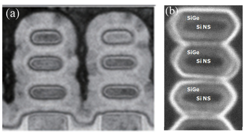
After more than five decades, Moore's Law for transistors is approaching the end of the international technology roadmap of semiconductors (ITRS). The fate of complementary metal oxide semiconductor (CMOS) architecture has become increasingly unknown. In this era, 3D transistors in the form of gate-all-around (GAA) transistors are being considered as an excellent solution to scaling down beyond the 5 nm technology node, which solves the difficulties of carrier transport in the channel region which are mainly rooted in short channel effects (SCEs). In parallel to Moore, during the last two decades, transistors with a fully depleted SOI (FDSOI) design have also been processed for low-power electronics. Among all the possible designs, there are also tunneling field-effect transistors (TFETs), which offer very low power consumption and decent electrical characteristics. This review article presents new transistor designs, along with the integration of electronics and photonics, simulation methods, and continuation of CMOS process technology to the 5 nm technology node and beyond. The content highlights the innovative methods, challenges, and difficulties in device processing and design, as well as how to apply suitable metrology techniques as a tool to find out the imperfections and lattice distortions, strain status, and composition in the device structures.
Keywords: CMOS; FDSOI; GAA; TFET; nanoscale transistors; process integration.
Conflict of interest statement
Hushan Cui is employed in Jiangsu Leuven Instruments Co., Ltd. The authors declare no conflicts of interest.
Figures


References
-
- Radamson H., Simoen E., Luo J., Zhao C. CMOS Past, Present and Future. Woodhead Publishing; Cambridge, UK: 2018.
-
- Jebalin B.K., Ajayan J., Franklin S.A., Nirmal D. A new Vertical C-shaped Silicon Channel Nanosheet FET with Stacked High-K Dielectrics for Low Power Applications. Silicon. 2024;16:2659–2670.
-
- Rezgui H., Wang Y., Mukherjee C., Deng M., Maneux C. Signature of electrothermal transport in 18nm vertical junctionless gate-all-around nanowire field effect transistors. J. Phys. D Appl. Phys. 2024 doi: 10.1088/1361-6463/ad4716. - DOI
Publication types
Grants and funding
- 2021ZD0302301/Innovation Program for Quantum Science and Technology
- 2017ZX02315001-002/National Key Project of Science and Technology of China
- Y7YC01X001/Academy of Integrated Circuit Innovation
- No.2020037/Youth Innovation Promotion Association of CAS
- 92064002/Nationl Natural Science Foundation of China
LinkOut - more resources
Full Text Sources
Miscellaneous
