

Programmable quantum emitter formation in silicon
- PMID: 38802357
- PMCID: PMC11130136
- DOI: 10.1038/s41467-024-48714-2
Programmable quantum emitter formation in silicon
Abstract
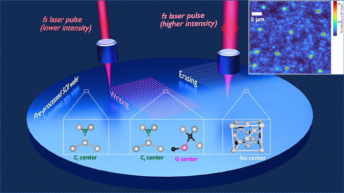
Silicon-based quantum emitters are candidates for large-scale qubit integration due to their single-photon emission properties and potential for spin-photon interfaces with long spin coherence times. Here, we demonstrate local writing and erasing of selected light-emitting defects using femtosecond laser pulses in combination with hydrogen-based defect activation and passivation at a single center level. By choosing forming gas (N2/H2) during thermal annealing of carbon-implanted silicon, we can select the formation of a series of hydrogen and carbon-related quantum emitters, including T and Ci centers while passivating the more common G-centers. The Ci center is a telecom S-band emitter with promising optical and spin properties that consists of a single interstitial carbon atom in the silicon lattice. Density functional theory calculations show that the Ci center brightness is enhanced by several orders of magnitude in the presence of hydrogen. Fs-laser pulses locally affect the passivation or activation of quantum emitters with hydrogen for programmable formation of selected quantum emitters.
© 2024. This is a U.S. Government work and not under copyright protection in the US; foreign copyright protection may apply.
Conflict of interest statement
The authors declare no competing interests.
Figures

Similar articles
-
Computationally Driven Discovery of T Center-like Quantum Defects in Silicon.J Am Chem Soc. 2024 Nov 6;146(44):30046-30056. doi: 10.1021/jacs.4c06613. Epub 2024 Oct 28. J Am Chem Soc. 2024. PMID: 39466834
-
Design for Telecom-Wavelength Quantum Emitters in Silicon Based on Alkali-Metal-Saturated Vacancy Complexes.ACS Nano. 2025 Feb 11;19(5):5418-5428. doi: 10.1021/acsnano.4c13620. Epub 2025 Jan 28. ACS Nano. 2025. PMID: 39873380
-
High-throughput identification of spin-photon interfaces in silicon.Sci Adv. 2023 Oct 6;9(40):eadh8617. doi: 10.1126/sciadv.adh8617. Epub 2023 Oct 4. Sci Adv. 2023. PMID: 37792930 Free PMC article.
-
Hexagonal Boron Nitride Quantum Simulator: Prelude to Spin and Photonic Qubits.ACS Nano. 2024 Aug 27;18(34):22609-22619. doi: 10.1021/acsnano.4c04240. Epub 2024 Aug 13. ACS Nano. 2024. PMID: 39138124 Free PMC article. Review.
-
Ultrafast optical control of individual quantum dot spin qubits.Rep Prog Phys. 2013 Sep;76(9):092501. doi: 10.1088/0034-4885/76/9/092501. Epub 2013 Sep 4. Rep Prog Phys. 2013. PMID: 24006335 Review.
Cited by
-
Solid-state single-photon sources operating in the telecom wavelength range.Nanophotonics. 2025 May 5;14(11):1729-1774. doi: 10.1515/nanoph-2024-0747. eCollection 2025 Jun. Nanophotonics. 2025. PMID: 40470101 Free PMC article. Review.
-
Photoactivation of Color Centers Induced by CW Laser Irradiation in Ion-Implanted Diamond.ACS Photonics. 2025 Jul 1;12(7):3803-3814. doi: 10.1021/acsphotonics.5c00826. eCollection 2025 Jul 16. ACS Photonics. 2025. PMID: 40688186 Free PMC article.
-
Enhanced zero-phonon line emission from an ensemble of W centers in circular and bowtie Bragg grating cavities.Nanophotonics. 2024 Nov 19;14(11):1939-1948. doi: 10.1515/nanoph-2024-0485. eCollection 2025 Jun. Nanophotonics. 2024. PMID: 40470082 Free PMC article.
References
-
- Baron Y, et al. Detection of single W-centers in silicon. ACS Photonics. 2022;9:2337–2345. doi: 10.1021/acsphotonics.2c00336. - DOI
-
- Redjem W, et al. Single artificial atoms in silicon emitting at telecom wavelengths. Nat. Electron. 2020;3:738–743. doi: 10.1038/s41928-020-00499-0. - DOI
-
- Quard, H. et al. Femtosecond-laser-induced creation of G and W color centers in silicon-on-insulator substrates. Phy. Rev. Appl. 21, 044014 (2024).
-
- Andrini, G. et al. Activation of telecom emitters in silicon upon ion implantation and ns pulsed laser annealing. Commun. Mater.5, 47 (2024).
