. 2024 May 28;15(1):4534.
doi: 10.1038/s41467-024-48631-4.

Domain wall magnetic tunnel junction-based artificial synapses and neurons for all-spin neuromorphic hardware

Affiliations

Domain wall magnetic tunnel junction-based artificial synapses and neurons for all-spin neuromorphic hardware

Long Liu et al. Nat Commun. .

Abstract

We report a breakthrough in the hardware implementation of energy-efficient all-spin synapse and neuron devices for highly scalable integrated neuromorphic circuits. Our work demonstrates the successful execution of all-spin synapse and activation function generator using domain wall-magnetic tunnel junctions. By harnessing the synergistic effects of spin-orbit torque and interfacial Dzyaloshinskii-Moriya interaction in selectively etched spin-orbit coupling layers, we achieve a programmable multi-state synaptic device with high reliability. Our first-principles calculations confirm that the reduced atomic distance between 5d and 3d atoms enhances Dzyaloshinskii-Moriya interaction, leading to stable domain wall pinning. Our experimental results, supported by visualizing energy landscapes and theoretical simulations, validate the proposed mechanism. Furthermore, we demonstrate a spin-neuron with a sigmoidal activation function, enabling high operation frequency up to 20 MHz and low energy consumption of 508 fJ/operation. A neuron circuit design with a compact sigmoidal cell area and low power consumption is also presented, along with corroborated experimental implementation. Our findings highlight the great potential of domain wall-magnetic tunnel junctions in the development of all-spin neuromorphic computing hardware, offering exciting possibilities for energy-efficient and scalable neural network architectures.


Conflict of interest statement

The authors declare no competing interests.

Figures

Fig. 1
Fig. 1. iDMI dependence on thickness of heavy metal layer.
a OOP magnetic hysteresis loops of W(t)/CFB(0.9)/MgO(2)/W(3)/Ru(2) film stack measured by VSM. The arrows indicate field sweeping direction. b Ku, Ms dependence on tW derived from VSM data in a. c AHE loops with read DC I = ± 8 mA and an in-plane bias field of Hx =  −1584 Oe. Inset shows the measurement schematic. d Hzeff as function of I under different Hx. e SOT efficiency χ versus Hx, and f iDMI constant obtained from samples with different tW, the corresponding error bars associated were defined experimentally. Inset shows experimentally measured D in W/CFB heterojunctions adapted from literature reports. The dash line is for guidance of eyes.
Fig. 2
Fig. 2. First principles calculations of iDMI in W/CoFe heterojunction.
a Schematic diagram of three sites mechanism of iDMI (left panel) and crystal structure of W/CoFe bilayer (right panel). b Plane-averaged electron difference density Δρ(r) (per unit cell) showing the charge transfer in CoFe/W structure with different tw. c Gain (peak1) and loss (peak2) of electron peaks extracted from b with difference W thickness. d Theoretically calculated D dependence on W thickness.
Fig. 3
Fig. 3. p-MTJ film stacks characterization, devices fabrication and testing.
a Schematic of PMA film stack, and b corresponding HRTEM bright-field (BF) and HAADF images. c OOP and IP M-H loops measured by VSM. Inset shows magnified loops at low fields. d Magnetoresistance versus Hz of p-MTJ device.
Fig. 4
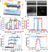
Fig. 4. Spin-synapse devices based-on DW-pMTJs.
a Schematic diagram of measurement configuration of four-state synaptic device, representative MOKE image of State III enclosure with magnified PCs. b TEM images of etched profiles at PC edge transition and bottom regions and the corresponding HRTEM image in PC bottom with inverse FFT patterns. c K-H (purple-green) and R-H (blue-red) loops as a function of Hz swept (forth-back) from pristine device before PCs formation. Blue curve denotes Kerr signal measured by p-MOKE. Colorful arrows represent respective magnetization orientation of PL, RF, FL at different states. d R-H loop as a function of Hz of the synaptic device with PCs. Dashed arrows illustrate sweep direction of Hz. e Magnified R-H loop as marked by green dash-box in d. f State-by-state switching of developed four-state synaptic device. Red, green and blue curves signify state1 (I) to state2 (II), state1 (I) to state3 (III), state1 (I) to state4 (IV) switching, respectively.
Fig. 5
Fig. 5. Spin-neuron based on DW-pMTJ sigmoidal activation function generator.
a MOKE image, the measuring configuration and protocol of spintronic sigmoid neuron based on DW-pMTJ. b Different resistance states with corresponding DW position. The green arrows indicate the state switching direction. Inset illustrates the resistance curve vs sweeping Hz. c Resistance as a function of Hz of sigmoidal device with central top electrode covering the whole channel (inset image). The arrows indicate field sweeping direction. d Resistance as a function of the amplitude and numbers of pulsed magnetic field for sigmoidal device in c. Insets depict the correspond array and magnified photos of the DW-pMTJ sigmoidal devices.
Fig. 6
Fig. 6. SOT and iDMI synergistic effect on DW dynamics with quantitative visualization.
a Schematic of proposed DW pinning mechanism with DMI profile. b Effective fields (left) and torques (right) in FM where mDW (green), DL (red), DMI (yellow), DWE (blue) denote center magnetization of domain wall, damping-like term of SOT effect, domain wall energy and iDMI, respectively. c Quantitative determination and illustration of DW motion and energy landscape with and without Je. Inset depicts the schematic of DW coordinates of q and φ.
Fig. 7
Fig. 7. Circuit simulation and experimental verification of spin neuron circuit.
a Schematic of a simplified ANN network comprising 16×16 DW-MTJ synapses and 16×1 16-state DW-MTJ neurons. b. Transient simulation results of the spin neuron circuit. c Hardware implementation of with developed 4 binary SOT-MTJs as synapse and 1 spin-neuron device (right panel). d Waveform of the pre-neuron signal output by MCU and corresponding output of the operational amplifier. e MOKE Kerr images captured after each pre-neuron signal applied.

References

    1. Ielmini D, Wong HSP. In-memory computing with resistive switching devices. Nat. Electron. 2018;1:333–343. doi: 10.1038/s41928-018-0092-2. - DOI
    1. Zhang W, et al. Neuro-inspired computing chips. Nat. Electron. 2020;3:371–382. doi: 10.1038/s41928-020-0435-7. - DOI
    1. Schuman CD, et al. Opportunities for neuromorphic computing algorithms and applications. Nat. Comput. Sci. 2022;2:10–19. doi: 10.1038/s43588-021-00184-y. - DOI - PubMed
    1. Zhou J, Chen J. Prospect of spintronics in neuromorphic computing. Adv. Electron. Mater. 2021;7:2100465. doi: 10.1002/aelm.202100465. - DOI
    1. Ross A, et al. Multilayer spintronic neural networks with radiofrequency connections. Nat. Nanotechnol. 2023;18:1273–1280. doi: 10.1038/s41565-023-01452-w. - DOI - PubMed