Light-Mediated Contact Printing of Phosphorus Species onto Silicon Using Carbene-Based Molecular Layers
- PMID: 38814003
- PMCID: PMC11171451
- DOI: 10.1021/acs.langmuir.4c00763
Light-Mediated Contact Printing of Phosphorus Species onto Silicon Using Carbene-Based Molecular Layers
Abstract
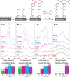
The ability to deposit pattern-specific molecular layers onto silicon with either regional p-/n-doping properties or that act as chemoselective resists for area-selective deposition is highly sought after in the bottom-up manufacturing of microelectronics. In this study, we demonstrate a simple protocol for the covalent attachment and patterning of a phosphorus-based dopant precursor onto silicon(100) functionalized with reactive carbene species. This method relies on selective surface reactions, which provide terminal functionalities that can be photochemically modified via ultraviolet-assisted contact printing between the carbene-functionalized substrate and an elastomeric stamp inked with the inorganic dopant precursor. X-ray photoelectron spectroscopy (XPS) analysis combined with scanning electron microscopy (SEM) imaging was used to characterize the molecule attachment and patterning ability of this technique. XPS spectra are indicative of the covalent bonding between phosphorus-containing molecules and the functionalized surface after both bulk solution-phase reaction and photochemical printing. SEM analysis of the corresponding printed features demonstrates the effective transfer of the phosphorus species in a patterned orientation matching that of the stamp pattern. This simple approach to patterning dopant precursors has the potential to inform the continued refinement of thin-film electronic, photonic, and quantum device manufacturing.
Conflict of interest statement
The authors declare no competing financial interest.
Figures


Similar articles
-
Erratum: Preparation of Poly(pentafluorophenyl acrylate) Functionalized SiO2 Beads for Protein Purification.J Vis Exp. 2019 Apr 30;(146). doi: 10.3791/6328. J Vis Exp. 2019. PMID: 31038480
-
Microcontact printing onto oxide-free silicon via highly reactive acid fluoride-functionalized monolayers.Small. 2010 Mar 8;6(5):642-50. doi: 10.1002/smll.200901650. Small. 2010. PMID: 20143349
-
Soft lithographic functionalization and patterning oxide-free silicon and germanium.J Vis Exp. 2011 Dec 16;(58):3478. doi: 10.3791/3478. J Vis Exp. 2011. PMID: 22214997 Free PMC article.
-
Photoresist Contact Patterning of Quantum Dot Films.ACS Nano. 2018 Oct 23;12(10):10024-10031. doi: 10.1021/acsnano.8b04462. Epub 2018 Sep 24. ACS Nano. 2018. PMID: 30247027
-
Double-Sided Opportunities Using Chemical Lift-Off Lithography.Acc Chem Res. 2016 Aug 16;49(8):1449-57. doi: 10.1021/acs.accounts.6b00034. Epub 2016 Apr 11. Acc Chem Res. 2016. PMID: 27064348
References
-
- Ogunfowora L. A.; Singh I.; Arellano N.; Pattison T. G.; Magbitang T.; Nguyen K.; Ransom B.; Lionti K.; Nguyen S.; Topura T.; Delenia E.; Sherwood M.; Savoie B. M.; Wojtecki R. Reactive Vapor-Phase Inhibitors for Area-Selective Depositions at Tunable Critical Dimensions. ACS Appl. Mater. Inter 2024, 16 (4), 5268–5277. 10.1021/acsami.3c14821. - DOI - PubMed
-
- Sánchez-Bodón J.; Andrade del Olmo J.; Alonso J. M.; Moreno-Benítez I.; Vilas-Vilela J. L.; Pérez-Alvarez L. Bioactive Coatings on Titanium: A Review on Hydroxylation, Self-Assembled Monolayers (SAMs) and Surface Modification Strategies. Polymers 2022, 14 (1), 165.10.3390/polym14010165. - DOI - PMC - PubMed
LinkOut - more resources
Full Text Sources

