Review
. 2024 Aug;11(29):e2402471.
doi: 10.1002/advs.202402471. Epub 2024 Jun 3.

Defects of Metal Halide Perovskites in Photocatalytic Energy Conversion: Friend or Foe?

Affiliations
Review

Defects of Metal Halide Perovskites in Photocatalytic Energy Conversion: Friend or Foe?

Chunhua Wang et al. Adv Sci (Weinh). 2024 Aug.

Abstract

Photocatalytic solar-to-fuel conversion over metal halide perovskites (MHPs) has recently attracted much attention, while the roles of defects in MHPs are still under debate. Specifically, the mainstream viewpoint is that the defects are detrimental to photocatalytic performance, while some recent studies show that certain types of defects contribute to photoactivity enhancement. However, a systematic summary of why it is contradictory and how the defects in MHPs affect photocatalytic performance is still lacking. In this review, the innovative roles of defects in MHP photocatalysts are highlighted. First, the origins of defects in MHPs are elaborated, followed by clarifying certain benefits of defects in photocatalysts including optical absorption, charge dynamics, and surface reaction. Afterward, the recent progress on defect-related MHP photocatalysis, i.e., CO2 reduction, H2 generation, pollutant degradation, and organic synthesis is systematically discussed and critically appraised, putting emphasis on their beneficial effects. With defects offering peculiar sets of merits and demerits, the personal opinion on the ongoing challenges is concluded and outlining potentially promising opportunities for engineering defects on MHP photocatalysts. This critical review is anticipated to offer a better understanding of the MHP defects and spur some inspiration for designing efficient MHP photocatalysts.

Keywords: charge dynamics; defect engineering; metal halide perovskites; solar‐to‐fuel conversion; surface reaction.


Conflict of interest statement

The authors declare no conflict of interest.

Figures

Figure 1
Figure 1
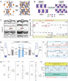
A) Comparison of the electronic band structure of traditional defect‐intolerant semiconductors (III‐V and II‐VI varieties) and defect‐tolerant MHPs. Reproduced with permission.[ 4b ] Copyright 2020, The Royal Society of Chemistry. B) Schematic illustration of hot‐carrier cooling below (left panel) and above (right panel) the multiple exciton generation (MEG) thresholds. Reproduced with permission.[ 4c ] Copyright 2018, The Authors, Published by Springer Nature. C) Schematic energy level diagram of typical MHPs. Reproduced with permission.[ 5 ] Copyright 2019, The Authors, Published by Springer Nature. D) Scheme of the charge recombination caused by defects. Reproduced with permission.[ 4b ] Copyright 2020, The Royal Society of Chemistry. E) Schematic illustration of the chlorine vacancy (VCl) in Cs2NaBiCl6 boosts the photocatalytic CO2 reduction. Reproduced with permission.[ 11a ] Copyright 2022, Wiley‐VCH.
Figure 2
Figure 2
Schematic diagram of the defect types in typical MAPbI3 material.
Figure 3
Figure 3
A–F) High‐resolution STM images of MAPbBr3. (A) Pristine surface, with MA+ molecules overlaid to show relative position. (B) An unpaired Br anion defect, (C) Two adjacent unpaired Br anion defects located near a vacancy. (D‐F) Single, double, and triple defects, respectively. Reproduced with permission.[ 22 ] Copyright 2019, American Chemical Society. (D, H) High‐resolution STM images of MAPbBr3. G) Dislocations, the start of dislocation rows indicated by the white arrow, and H) defect on the surface, inset: Height profile across a defect along the green line indicated in the image. Reproduced with permission.[ 21 ] Copyright 2015, American Chemical Society. I–K) Atomic‐resolution scanning transmission electron microscopy (STEM) of FAPbI3. (I) Native intergrowth between PbI2 (shaded yellow) and FAPbI3 formed. (J) Abrupt grain boundaries and (K) edge dislocations (green rectangle). Reproduced with permission.[ 23 ] Copyright 2020, The Authors, published by American Association for the Advancement of Science. L–P) TEM images of the degradation transition of MAPbI3 (L‐O) Pb‐cluster at the GBs during time, yellow circles indicate Pb‐clusters at the GBs. (P) Schematic showing the Pb nano‐clusters growing at the perovskite grain boundaries and leaving empty spaces behind as shown in Figure 4O. Reproduced with permission.[ 24 ] Copyright 2019, The Authors, published by Springer Nature.
Figure 4
Figure 4
A) The crystal structure of MAPbI3. Reproduced with permission.[ 40b ] Copyright 2015, American Chemical Society. B) Partial charge density at CBM (upper) and VBM (lower), C) Band structure, and D) Density of states of MAPbI3, from (i) to (iv) are total DOS and MA+, Pb, I partial DOS respectively, E) The formation energies of intrinsic point defects in MAPbI3 as a function of Fermi level at three chemical potential points, from (i) to (iii) are I‐rich/Pb‐poor, moderate and I‐poor/Pb‐rich conditions, respectively. F) Calculated transition energy levels of intrinsic acceptors (i) and intrinsic donors (ii) of MAPbI3. Reproduced with permission.[ 18 ] Copyright 2014, AIP Publishing. G) Density of the trap states of MAPbI3 single crystal extracted from temperature‐dependent SCLC technique. Reproduced with permission.[ 43 ] Copyright 2016, Wiley‐VCH.
Figure 5
Figure 5
A) The construction of the CBM and VBM in MHP materials with different halogens. B) The formation energies of intrinsic point defects in MAPbBr3 as a function of Fermi level at three chemical potential points, from (i) to (iii) are Br‐rich/Pb‐poor, moderate, and Br‐poor/Pb‐rich conditions, respectively. C) The transition energy levels of intrinsic donors (left) and intrinsic acceptors (right) of MAPbBr3. Reproduced with permission.[ 40a ] Copyright 2022, IOP Publishing. D) Calculated defect formation energies in the CsPbBr3 as a function of Fermi level, from left to right are Cs‐poor, moderate, and Br‐poor conditions, respectively. E) Calculated transition energy levels for vacancies and anti‐site defects of CsPbBr3. Reproduced with permission.[ 46 ] Copyright 2015. American Physical Society.
Figure 6
Figure 6
A) Atomic structure changes before (upper) and after (lower) the formation of a Pb dimer via VI. B) Band structure changes for VI before (left) and after (right) the formation of Pb dimer. C) Atomic structure changes before (upper) and after (lower) the formation of an I trimer via IMA. D) Band structure changes for IMA before (left) and after (right) the formation of I trimer. Reproduced with permission.[ 50 ] Copyright 2014, American Chemical Society. E) Defect pair representation in FAPbI3. F) Calculated charge transition energy levels of defect pairs, the letter X in each box at the top represents one of the six donor defects to be paired with the corresponding acceptor defect in the same box. Reproduced with permission.[ 53 ] Copyright 2022, American Chemical Society.
Figure 7
Figure 7
Structures of Pb‐based ABX3 perovskite and common lead‐free perovskite derivates.
Figure 8
Figure 8
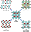
A) Crystalline phase variation of Cs3Bi2I9 (0D dimer phase) and Rb3Bi2I9 (2D layered phase). Reproduced with permission.[ 69a ] Copyright 2015, American Chemical Society. B) Cl‐induced phase transformation from the 0D dimer phase of A3Sb2I9 to the 2D layered phase of A3Sb2Cl x I9– x . Reproduced with permission.[ 70 ] Copyright 2018, American Chemical Society. C) Calculated band structures of Cs3Sb2I9 in layered and dimer modifications. D) Calculated transition energy levels of intrinsic donors (red lines) and acceptors (blue lines) in Cs3Sb2I9. Reproduced with permission.[ 71 ] Copyright 2015, American Chemical Society. E) Schematic molecular orbital diagrams Cs2AgBiCl6 (left) and Cs2AgBiBr6 (right). The dark blue and the gray rectangles correspond to the Bi‐halide hybrid bands and the Ag‐halide hybrid bands, respectively. The light blue rectangles represent the bands formed in Cs2AgBiCl6 and Cs2AgBiBr6, respectively. Filled rectangles represent occupied (valence) bands and empty rectangles represent the unoccupied (conduction) bands. Reproduced with permission.[ 80a ] Copyright 2016, American Chemical Society. F) Calculated transition energy levels of intrinsic acceptors (upper) and donors (lower) in Cs2AgBiBr6. Reproduced with permission.[ 81 ] Copyright 2016, Wiley‐VCH. G) The band structure of Cs2SnX6 predicted by the molecular orbital theory, (i) Cs2SnI6, (ii) Cs2SnBr6, and (iii) Cs2SnCl6. Reproduced with permission.[ 82 ] Copyright 2019, American Chemical Society. H) Calculated transition energy levels for intrinsic defects in Cs2SnI6. Donor states are marked with red lines and acceptor states are denoted by blue lines. Reproduced with permission.[ 88 ] Copyright 2015, Royal Society of Chemistry.
Figure 9
Figure 9
A) UV‐vis absorption spectra of TiO2 with and without hydrogen‐mediated oxygen vacancies (OVH). Inset shows the digital photos of the materials. Reproduced with permission.[ 93 ] Copyright 2018, Wiley‐VCH. B) Schematic illustration of the band structure of In2O3 and VO‐rich In2O3. Reproduced with permission.[ 94 ] Copyright 2014, American Chemical Society. C) UV‐vis absorption spectra of Cs2AgBiBr6 and Br defect‐rich Cs2AgBiBr6. Reproduced with permission.[ 11e ] Copyright 2021, American Chemical Society. D) Band edge positions of Cs2NaBiCl6 with and without Cl vacancies. Reproduced with permission.[ 11a ] Copyright 2022, Wiley‐VCH.
Figure 10
Figure 10
A) Electrochemical impedance spectra of Bi2WO6 (BWO) and VO‐PO4‐BWO. Reproduced with permission.[ 102 ] Copyright 2016, Elsevier. B) Linear sweep voltammetry curves of TiO2 and defect‐engineered TiO2 in the TiO2/Bi2WO6 systems. Reproduced with permission.[ 103 ] Copyright 2017, Elsevier. C) Transient photocurrent response of Cs2AgBiBr6 and the samples with Cs vacancies. Reproduced with permission.[ 11f ] Copyright 2022, Elsevier. D) Surface photovoltage of Cs2NaBiCl6 and Cl‐vacancy rich Cs2NaBiCl6 samples. Reproduced with permission.[ 11a ] Copyright 2022, Wiley‐VCH.
Figure 11
Figure 11
The effect of defects on MHP materials and the applications of defect‐contained MHPs on various photoredox systems.
Figure 12
Figure 12
A) Photocatalytic performance of CO2 reduction over CsPbBr3, Br‐rich CsPbBr3, and their composites with g‐C3N4. Reproduced with permission.[ 8c ] Copyright 2022, American Chemical Society. B) Photocatalytic performance of toluene oxidation over Cs3Bi2Br9, Cs3Bi2Br9@BiOBr, and Cs3Bi2Br9@BiOBr/A‐SiO2. Reproduced with permission.[ 8d ] Copyright 2022 Wiley‐VCH. C) Summary of ligand modification of MHPs with different types of passivation ligands. Reproduced with permission.[ 8a ] Copyright 2022, American Chemical Society. D) Schematic illustration of defects passivation with various surface ligands. Reproduced with permission.[ 112 ] Copyright 2021, Wiley‐VCH.
Figure 13
Figure 13
A) Absorption spectra, B) Electrochemical impedance plots, C) Gibbs free energy profiles, and D) Photocatalytic performance of CO2 reduction over Cs2NaBiCl6 (‐H), chlorine vacancy Cs2NaBiCl6 (‐A) and Cs2NaBiCl6 (‐G), where H, A, and G represent the Cs2NaBiCl6 prepared using hydrothermal, annealing and grinding method. Reproduced with permission.[ 11a ] Copyright 2022, Wiley‐VCH. E) The relationship between photoreduction CO2 to CO and reduction free energy of the main reactions in the photocatalytic CO2 reduction processes over Cs3Bi2Br9 and Cs3Bi2Cl9 photocatalysts. Reproduced with permission.[ 118 ] Copyright 2020, American Chemical Society. F) Density of states plots of Cs2AgBiBr6 with and without Br‐vacancy. Reproduced with permission.[ 116 ] Copyright 2021, The authors, American Chemical Society. Published by MDPI. G) In‐situ EPR data of Cs3Sb2I9 in toluene under light irradiation. H) The photocatalytic performance of CO2 reduction over Cs3Sb2I9 under photo‐, thermo‐, and photothermal synergistic catalysis. I) Schematic illustration of CO2 reduction over Cs3Sb2I9 catalyst with the photothermal synergistic effect. Reproduced with permission.[ 11c ] Copyright 2021, Elsevier.
Figure 14
Figure 14
A) Scheme of the photocatalytic H2 evolution over the Br defect‐rich Cs2AgBiBr6 photocatalyst. B) H2 generation rate over Br‐rich Cs2AgBiBr6 and reference samples. Reproduced with permission.[ 11e ] Copyright 2021, American Chemical Society. C) The Gibbs free energy plots of CsPbBr3 with and without Br vacancies for photocatalytic H2 generation. D) The H2 production rate over pristine CsPbBr3 (3D NCs) and Br‐rich CsPbBr3 (1D NRs). Reproduced with permission.[ 122 ] Copyright 2023, Royal Society of Chemistry. E) Schematic illustration of the charge dynamics in MAPbI3 with and without the continuation of defective areas for solar‐driven H2 generation. F) H2 generation rate over MAPbI3‐I and MAPbI3‐C photocatalysts. Reproduced with permission.[ 11b ] Copyright 2023, Wiley‐VCH.
Figure 15
Figure 15
A) Schematic illustrating band structures of Cs2AgBiBr6 samples, where CABB‐ET‐0, 10, 20, and 30 represent adding of Ethylenediaminetetraacetic acid disodium salt (ET) with different evaporation time (0, 10, 20, and 30 min). B) Photodegradation performance of tetracycline over various Cs2AgBiBr6. C) The proposed mechanism for photodegradation of the tetracycline over CABB‐ET samples. Reproduced with permission.[ 11f ] Copyright 2022, Elsevier. D) Photocatalytic NO oxidation over Cs3Bi2− x Pb x Br9− x photocatalysts. Reproduced with permission.[ 100 ] Copyright 2023, The Authors, published by Springer.
Figure 16
Figure 16
A) UV‐Vis spectra of Cs3Bi2Br9 materials adsorbed with (red) and without alizarin (blue), and pure alizarin (black). B) Illustrating photocatalytic epoxide alcoholysis over Cs3Bi2Br9 sample with Lewis acid sites. Reproduced with permission.[ 126 ] Copyright 2019, Wiley‐VCH. C) Reaction energy profile of toluene oxidation over Cs3Bi2Br9 and CdS. (D‐E) Schematic illustration showing D) different key intermediates that adsorbed on Cs3Bi2Br9 surface and E) charge density difference of adsorbed intermediates. Reproduced with permission.[ 127 ] Copyright 2022, Elsevier.

References

    1. a) Xia C., Kirlikovali K. O., Nguyen T. H. C., Nguyen X. C., Tran Q. B., Duong M. K., Dinh M. T. N., Nguyen D. L. T., Singh P., Raizada P., Coord. Chem. Rev. 2021, 446, 214117;
    2. b) Wu X., Tan H. L., Zhang C., Teng Z., Liu Z., Ng Y. H., Zhang Q., Su C., Prog. Mater. Sci. 2022, 133, 101047;
    3. c) Ding Y., Maitra S., Halder S., Wang C., Zheng R., Barakat T., Roy S., Chen L.‐H., Su B.‐L., Matter 2022, 5, 2119.
    1. a) Qu S., Wu H., Ng Y. H., Adv. Energy Mater. 2023, 13, 2301047;
    2. b) Wang C., Zhang H., Lai F., Xie Z., Ng Y. H., Weng B., Wu X., Liao Y., J. Energy Chem. 2023, 83, 341;
    3. c) Ding Y., Wang C., Zheng R., Maitra S., Zhang G., Barakat T., Roy S., Su B.‐L., Chen L.‐H., EnergyChem 2022, 4, 100081.
    1. a) Peng S., Yang Z., Sun M., Yu L., Li Y., Adv. Mater. 2023, 35, 2304711; - PubMed
    2. b) Ding Y., Maitra S., Wang C., Zheng R., Zhang M., Barakat T., Roy S., Liu J., Li Y., Hasan T., Su B. L., J. Energy Chem. 2022, 70, 236.
    1. a) Wang C., Huang H., Weng B., Verhaeghe D., Keshavarz M., Jin H., Liu B., Xie H., Ding Y., Gao Y., Appl. Catal. B: Environ. 2022, 301, 120760;
    2. b) Jin H., Debroye E., Keshavarz M., Scheblykin I. G., Roeffaers M. B., Hofkens J., Steele J. A., Mater.Horiz 2020, 7, 397;
    3. c) Li M., Begum R., Fu J., Xu Q., Koh T. M., Veldhuis S. A., Grätzel M., Mathews N., Mhaisalkar S., Sum T. C., Nat. Commun 2018, 9, 4197; - PMC - PubMed
    4. d) Wang C., Zhang C., Wang S., Liu G., Xia H., Tong S., He J., Niu D., Zhou C., Ding K., Sol. RRL 2018, 2, 1700209.
    1. Tao S., Schmidt I., Brocks G., Jiang J., Tranca I., Meerholz K., Olthof S., Nat. Commun. 2019, 10, 2560. - PMC - PubMed

LinkOut - more resources