Review
. 2024;100(6):320-334.
doi: 10.2183/pjab.100.022.

Optical coupling of individual air-suspended carbon nanotubes to silicon microcavities

Affiliations
Review

Optical coupling of individual air-suspended carbon nanotubes to silicon microcavities

Wataru Terashima et al. Proc Jpn Acad Ser B Phys Biol Sci. 2024.

Abstract

Carbon nanotubes are a telecom band emitter compatible with silicon photonics, and when coupled to microcavities, they present opportunities for exploiting quantum electrodynamical effects. Microdisk resonators demonstrate the feasibility of integration into the silicon platform. Efficient coupling is achieved using photonic crystal air-mode nanobeam cavities. The molecular screening effect on nanotube emission allows for spectral tuning of the coupling. The Purcell effect of the coupled cavity-exciton system reveals near-unity radiative quantum efficiencies of the excitons in carbon nanotubes.

Keywords: Purcell effect; carbon nanotubes; cavity quantum electrodynamics; microcavity; silicon photonics.


Figures
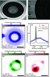
Fig. 1
Fig. 1
(Color online) (a) Scanning electron micrograph of an as-fabricated Si microdisk. (b) Scanning electron micrograph of a suspended nanotube attached to a microdisk. (c) A photoluminescence (PL) image of Si emission coupled to a whispering gallery mode (WGM), taken with λex=771 nm and P=1.5 mW. The spectra have been integrated from 1171 to 1175 nm to construct this image. (d) High-resolution PL spectrum of nanotube emission coupled to a WGM. Dots are data, and lines are Lorentzian fits. The peak values obtained from the fits are plotted in (e) and (f). (e) A PL intensity mapping for carbon nanotube (CNT) emission coupled to a WGM. (f) A PL intensity mapping for direct CNT emission, taken with λex=857 nm and P=0.3 mW with circular polarization. The scale bars in the images are 2 μ m. The dotted circles in (c), (e), and (f) represent the Si microdisk. Original data are presented in Ref. 24.
Fig. 2
Fig. 2
(a, b) Scanning electron micrographs of (a) dielectric- and (b) air-mode photonic crystal nanobeam cavities, respectively. (c, d) Profiles of normalized y -component of electric fields Ey at z=130 nm. The origin of the coordinate system is the center of the cavity. For (c), a dielectric-mode cavity with a=390 nm, cavity-center period of 0.84a , and 200 nm by 530 nm holes is used for the calculation. For (d), an air-mode cavity with a=430 nm, cavity-center period of 1.16a , and 220 nm by 510 nm holes is used. Panels (a–d) share the 2 μ m scale bar in (a). (e) A schematic of a device with an individual carbon nanotube (CNT). (f) Scanning electron micrograph of a device with a suspended nanotube. The scale bar is 2 μ m. (g) Typical photoluminescence (PL) spectrum of an air-mode device coupled to a nanotube. The dots are data, and the lines are Lorentzian fits. Original data are presented in Ref. 25.
Fig. 3
Fig. 3
(Color online) Spatial distribution of nanotubes that show coupling. (a, b) Spatial distribution of photoluminescence (PL) peak intensity locations for dielectric- and air-mode cavities. The peak locations are determined by two-dimensional Gaussian fitting, and they are plotted as a function of the displacement from the center of the cavity. The center of the cavities is taken as the origin of the coordinate system. Original data are presented in Ref. 25.
Fig. 4
Fig. 4
(a) Excitation power dependence of photoluminescence (PL). PL is normalized with respect to the nanotube peak height. Vertical dashed lines indicate the powers where PL spectra in (b) are taken. (b) Comparison of PL spectra taken at P=200 μ W (orange) and 300 μ W (green). (c, d) Excitation power dependence of the (c) peak center energy and (d) peak area. Red open circles are obtained from the CNT peak, and the blue dots are taken from the cavity emission. The peak center energies are plotted as the difference from the resonant energy ωcav=1.018  eV. For (a–d), excitation laser energy is tuned to E22 resonance, and laser polarization is perpendicular to the nanobeam. (e, f) Excitation power dependence of (e) F and (f) S . (g) F as a function of S . Open circles indicate red-detuned nanotube emission conditions ( P190 μ W), and crosses correspond to blue-detuned conditions ( P>190 μ W). Original data are presented in Ref. 26.
Fig. 5
Fig. 5
(a) Schematic of the device. (b) Scanning electron micrograph of a fabricated device. A carbon nanotube (CNT) is suspended across the width of the trench near the center of the image. The scale bar is 1 μ m. (c) Typical photoluminescence (PL) spectrum of a device showing optical coupling to the cavity. The dots are data, and the gray line is the bi-Lorentzian fit. The blue and red curves correspond to the cavity and CNT peak components, respectively. We interpret the asymmetry of the peak shape as a dip caused by the interference of the optics or the interference with the reflection from the bottom of the nanobeam substrate. λex=793 nm and P=20 μ W are used for the excitation, and the laser polarization is parallel to the nanotube axis. Original data are presented in Ref. 27.
Fig. 6
Fig. 6
(a) Calculated far-field radiation pattern of the fundamental cavity mode. (b) Calculated far-field radiation pattern of the uncoupled nanotube emission. For (a) and (b), photon flux density is plotted as a function of polar and azimuthal angles in spherical coordinates. The radial axis represents the polar angle. The green circle represents the numerical aperture of the objective lens. (c) Decay curves for (blue) the Purcell-enhanced nanotube emission from the same device as in Fig. 5(c) and (red) a 2.0- μ m-long (9,8) nanotube in free space. The excitation powers are 100 and 5 nW for nanotubes in the cavity and free space, respectively. (d, e) Length dependence of (d) τ1 and (e) τ2 in free space. The red dots are data, and the lines are fits using the exciton diffusion model. The blue dashed line in (d) shows the dark exciton lifetime in the cavity, from which we extract the effective nanotube length. The blue triangle in (e) shows the Purcell-accelerated bright exciton lifetime. Original data are presented in Ref. 27.
Fig. 7
Fig. 7
(Color online) The acceleration factor as a function of the Purcell factor. The dots are data, and the error bars show the 1 σ confidence interval. The line indicates η=1 as given by Eq. [7]. Chiralities of the nanotubes in the measured devices are (9,7), (9,8), (10,8), and (11,6). Original data are presented in Ref. 27.

Similar articles

References

    1. Thomson D., Zilkie A., Bowers J. E., Komljenovic T., Reed G. T., Vivien L., et al. (2016) Roadmap on silicon photonics. J. Opt. 18, 073003.
    1. Wang Z., Abbasi A., Dave U., De Groote A., Kumari S., Kunert B., et al. (2017) Novel light source integration approaches for silicon photonics. Laser Photon. Rev. 11, 1700063.
    1. Kong J., Soh H. T., Cassell A. M., Quate C. F., Dai H. (1998) Synthesis of individual single-walled carbon nanotubes on patterned silicon wafers. Nature 395, 878-881.
    1. O'Connell M. J., Bachilo S. M., Huffman C. B., Moore V. C., Strano M. S., Haroz E. H., et al. (2002) Band gap fluorescence from individual single-walled carbon nanotubes. Science 297, 593-596. - PubMed
    1. Weisman R. B., Bachilo S. M. (2003) Dependence of optical transition energies on structure for single-walled carbon nanotubes in aqueous suspension: An empirical Kataura plot. Nano Lett. 3, 1235-1238.