. 2024 May 28;29(11):2533.
doi: 10.3390/molecules29112533.

Dual Optoelectronic Organic Field-Effect Device: Combination of Electroluminescence and Photosensitivity

Affiliations

Dual Optoelectronic Organic Field-Effect Device: Combination of Electroluminescence and Photosensitivity

Vasiliy A Trukhanov et al. Molecules. .

Abstract

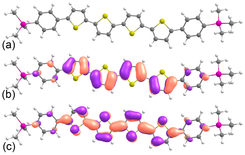
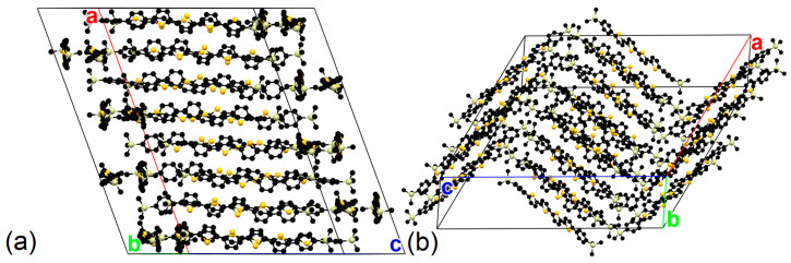
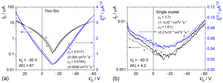
Merging the functionality of an organic field-effect transistor (OFET) with either a light emission or a photoelectric effect can increase the efficiency of displays or photosensing devices. In this work, we show that an organic semiconductor enables a multifunctional OFET combining electroluminescence (EL) and a photoelectric effect. Specifically, our computational and experimental investigations of a six-ring thiophene-phenylene co-oligomer (TPCO) revealed that this material is promising for OFETs, light-emitting, and photoelectric devices because of the large oscillator strength of the lowest-energy singlet transition, efficient luminescence, pronounced delocalization of the excited state, and balanced charge transport. The fabricated OFETs showed a photoelectric response for wavelengths shorter than 530 nm and simultaneously EL in the transistor channel, with a maximum at ~570 nm. The devices demonstrated an EL external quantum efficiency (EQE) of ~1.4% and a photoelectric responsivity of ~0.7 A W-1, which are among the best values reported for state-of-the-art organic light-emitting transistors and phototransistors, respectively. We anticipate that our results will stimulate the design of efficient materials for multifunctional organic optoelectronic devices and expand the potential applications of organic (opto)electronics.

Keywords: charge transport; density functional theory; electroluminescence; light-emitting transistors; organic field-effect transistors; organic phototransistors; organic semiconductors; thiophene-phenylene co-oligomers.


Conflict of interest statement

The authors declare no conflicts of interest.

Figures

Figure 1
Figure 1
Calculated equilibrium geometry (a), HOMO (b) and LUMO (c) patterns of TMS-P4TP-TMS molecule. Hydrogen atoms are shown in white, carbon in grey, sulfur in yellow, and silicon in purple.
Figure 2
Figure 2
Crystal structure of TMS-P4TP-TMS in two projections: view on the herringbone motif (a) and on the layered packing (b). Black spheres denote carbon atoms, yellow spheres denote sulfur atoms, and white spheres denote silicon atoms; hydrogen atoms are not shown, a, b, and c are the lattice vectors.
Figure 3
Figure 3
Charge transport directions for electrons (a) and holes (b) in the TMS-P4TP-TMS crystal; all the presented molecules belong to the same molecular layer. The thickness of the arrows connecting various molecules depicts the magnitude of the corresponding transfer integrals; the latter are also labeled (in meV). Transfer integrals below 5 meV are shown with dashed lines and are not labeled. Arrows in the left bottom corners of the panels denote the lattice vectors a, b, and c.
Figure 4
Figure 4
Transfer characteristics for thin-film (a) and single-crystal (b) OFET. Blue lines denote the transfer characteristics in terms of square root of the drain current.
Figure 5
Figure 5
(a) Image of thin-film OLET, EL image (orange) was captured at an exposure of 18 s, while gate voltage VG was changed from –12 to –8 V with step 0.5 V (9 points) at drain voltage VD = –30 V. The EL image is superimposed with the OLET image captured under backlight. Letters S and D denote source and drain electrodes, correspondingly. (b) Image of a single-crystal OLET with its EL image under operation. (c) EL spectra of thin-film (TF) and single-crystal (SC) OLETs, PL, and absorption spectra of TMS-P4TP-TMS in thin film and in solution (spectra in solution are represented in Ref. [27]). (d) Drain current ID and EL EQE versus VG for the thin-film OLET. Original images of OLETs under backlight and in dark are given in Supplementary Materials, Figure S9.
Figure 6
Figure 6
Photoelectric effect in the thin-film devices: (a) typical drain current, ID, vs time at constant drain and gate voltages under chopped incident illumination, (b) normalized photocurrent, Iph/ID, vs the gate voltage at VD = –20 V, (c) responsivity spectrum at VG = –30 V and VD = –40 V (blue solid line); the EL spectrum (red dashed line) taken from Figure 5c is shown for reference, (d) normalized photocurrent as a function of the incident optical power at λ = 530 nm, VD = –20 V and VG = –10 V; the red line is a fit to the experimental data with a logarithmic function.

Similar articles

References

    1. Liao C., Yan F. Organic Semiconductors in Organic Thin-Film Transistor-Based Chemical and Biological Sensors. Polym. Rev. 2013;53:352–406. doi: 10.1080/15583724.2013.808665. - DOI
    1. Wang Y., Zhang J., Zhang S., Huang J. OFET chemical sensors: Chemical sensors based on ultrathin organic field-effect transistors. Polym. Int. 2021;70:414–425. doi: 10.1002/pi.6095. - DOI
    1. Muccini M. A bright future for organic field-effect transistors. Nat. Mater. 2006;5:605–613. doi: 10.1038/nmat1699. - DOI - PubMed
    1. Chaudhry M.U., Muhieddine K., Wawrzinek R., Sobus J., Tandy K., Lo S.-C., Namdas E.B. Organic Light-Emitting Transistors: Advances and Perspectives. Adv. Funct. Mater. 2020;30:1905282. doi: 10.1002/adfm.201905282. - DOI
    1. Baeg K.-J., Binda M., Natali D., Caironi M., Noh Y.-Y. Organic Light Detectors: Photodiodes and Phototransistors. Adv. Mater. 2013;25:4267–4295. doi: 10.1002/adma.201204979. - DOI - PubMed

LinkOut - more resources