. 2024 Jun 19;15(1):5252.
doi: 10.1038/s41467-024-49399-3.

Direct bandgap quantum wells in hexagonal Silicon Germanium

Affiliations

Direct bandgap quantum wells in hexagonal Silicon Germanium

Wouter H J Peeters et al. Nat Commun. .

Abstract

Silicon is indisputably the most advanced material for scalable electronics, but it is a poor choice as a light source for photonic applications, due to its indirect band gap. The recently developed hexagonal Si1-xGex semiconductor features a direct bandgap at least for x > 0.65, and the realization of quantum heterostructures would unlock new opportunities for advanced optoelectronic devices based on the SiGe system. Here, we demonstrate the synthesis and characterization of direct bandgap quantum wells realized in the hexagonal Si1-xGex system. Photoluminescence experiments on hex-Ge/Si0.2Ge0.8 quantum wells demonstrate quantum confinement in the hex-Ge segment with type-I band alignment, showing light emission up to room temperature. Moreover, the tuning range of the quantum well emission energy can be extended using hexagonal Si1-xGex/Si1-yGey quantum wells with additional Si in the well. These experimental findings are supported with ab initio bandstructure calculations. A direct bandgap with type-I band alignment is pivotal for the development of novel low-dimensional light emitting devices based on hexagonal Si1-xGex alloys, which have been out of reach for this material system until now.


Conflict of interest statement

The authors declare no competing interests.

Figures

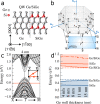
Fig. 1
Fig. 1. Quantum wells of hex-Ge/Si0.2Ge0.8.
a Schematic illustration of the GaAs/Si0.2Ge0.8/Ge/Si0.2Ge0.8 core-multishell nanowires. All interfaces are orthogonal to 11¯00 directions. b Schematic band alignment of the different materials. The electrons and holes are confined in the hex-Ge layer due to type-I alignment with the surrounding hex-Si0.2Ge0.8, as will be proven in this manuscript. Approximate values of the bandgap and offsets are given. c 30-degree tilted scanning electron micrograph of a NW array. Within these NWs, a (12 ± 3) nm Ge/Si0.2Ge0.8 QW is embedded.
Fig. 2
Fig. 2. Structural properties of the studied Ge/Si0.2Ge0.8 QWs.
a False-colored HAADF-STEM image of a cross-sectional lamella, viewing the Ge QW along the [0001] zone axis. Inset shows that Ge QWs on neighboring facets have different thicknesses. b Growth rate curve for Ge/Si0.2Ge0.8 QWs. The thicknesses of individual facets, all measured in images acquired along the [0001] zone axis, are indicated with the colored data points. Colored areas show approximate probability distributions, obtained from these data points by Kernel smoothing. c False-colored HAADF-STEM image of a cross-sectional lamella, viewing the QW along the [112¯0] zone axis. The core of the NW is on the left. Locations with local hexagonal (ABABA, blue), cubic (ABCA, green), and twinned cubic boundary (ABCBA, pink) stacking are indicated with circles. The pink arrow highlights a defect that starts in the Ge QW. d X-ray diffraction reciprocal space map around the hexagonal [101¯5] reflection. The peak position does not match Vegard’s rule (dashed line), indicating pseudomorphic strain relaxation.
Fig. 3
Fig. 3. Quantum confinement in hex-Ge/Si0.2Ge0.8 QWs.
a Ge/Si0.2Ge0.8 PL spectrum for varying growth time at low temperature (T ≈ 4 K) and low excitation density (P≤65 W cm−2), b The PL emission versus the QW thicknesses tQW determined from TEM, together with the confinement energy predicted from theory shifted up by 60 meV to account for the difference in the theoretical and experimental bandgap of the hex-Ge. The dashed line shows the confinement energies using a simple finite QW model. We also include the reference spectra of bulk-Ge and the bulk Si0.2Ge0.8 barrier as horizontal lines with the FWHM of the spectra shown as horizontal gray bars. Error bars in tQW are the standard deviations presented in Fig. 2b and error bars in the peak energy indicate the FWHM of the emission spectrum.
Fig. 4
Fig. 4. Type-I band alignment in hex-Ge/Si0.2Ge0.8 QWs.
a The (10 ± 4) nm (2.5 min) low temperature (T ≈ 4 K) QW photoluminescence spectrum as a function of excitation density showing a constant lineshape over two orders of magnitude with the peak position in between the bulk-Ge and Si0.2Ge0.8 barrier reference measurements, b The (10 ± 4) nm QW showing a near constant lineshape through temperature with the tail states becoming slightly more significant as the peak intensity quenches at higher temperatures. c The emission peak energy of the (10 ± 4) nm QW shows a nearly constant magnitude through excitation density. Initially the peak blueshifts due to band-filling of the QW and then redshift around 100 W cm−2, likely due to Bandgap renormalization. d The (24 ± 7) nm (9 min) QW spectrum evolves from a single to a double peak with increasing excitation density due to band-filling. Additionally, if the lowest and highest excitation density spectra are compared, we observe no significant shift in the position of the low energy peak. e The (24 ± 7) nm QW sample as a function of temperature showing emission up to room temperature. f The Arrhenius plot of the QWs and Si0.2Ge0.8 barrier reference samples measured at an excitation density of 0.88 kW cm−2. It can be seen that the temperature behavior of the QWs exceeds the bulk hex-Si0.2Ge0.8 reference. g The Light-In Light-Out (LILO) curves of the QWs and SiGe barrier reference samples measured at 4 K. The slopes of (0.69 ± 0.01) and (0.66 ± 0.01) for the (24 ± 7) nm and (10 ± 4) nm QWs respectively exceed the (0.59 ± 0.02) of the bulk hex-Si0.2Ge0.8 reference.
Fig. 5
Fig. 5. Studies of hex-Si0.1Ge0.9/Si0.3Ge0.7 QWs.
a False-colored HAADF-STEM of a cross-sectional lamella, viewing the (5 ± 1) nm (5 min) Si0.1Ge0.9/Si0.3Ge0.7 QW in the [0001] zone axis. b Background corrected photoluminescence spectra for varying QW growth time at low temperature ( ≈ 4 K) and high excitation density < 0.88 kW cm−2. Reference spectra of bulk Si0.1Ge0.9 and Si0.3Ge0.7 are included. c The PL emission versus the QW thicknesses tQW determined from TEM. Spectra of the Si0.1Ge0.9 well and Si0.3Ge0.7 barrier alloys are included as horizontal lines with the FWHM of the spectra as horizontal gray bars. A simple finite QW model is calculated for this heterostructure which shows reasonable agreement with the experiment. Error bars in tQW are the standard deviations presented in Fig. S7e and error bars in the peak energy indicate the FWHM of the emission spectrum. d Initial QW lifetime measured using TCSPC for the (5 ± 1) nm QW for varying laser fluence with the error bars indicating the standard deviation determined fitting the initial decays presented in Fig. S9b.
Fig. 6
Fig. 6. Band structure calculations of hex-Ge/Si0.25Ge0.75.
a Hexagonal Ge/Si0.25Ge0.75 heterostructure with (11¯00) interfaces. b Bulk hexagonal Brillouin zone (BZ) and its projection onto the two-dimensional BZ of the (11¯00) interface. c Direct bandgap band structure of hexagonal 4 nm Ge/ 2 nm Si0.25Ge0.75 multiple quantum well structure (black lines) and bulk Si0.25Ge0.75 (gray area) projected onto the two-dimensional Brillouin zone. The horizontal red line indicates the branching points of the two systems used as energy zero for alignment. d Energies of the lowest electron and highest hole subband at Γ¯ versus Ge thickness in the Ge/Si0.25Ge0.75 heterostructures studied. They are compared with the lowest conduction and highest valence band of the bulk Si0.25Ge0.75 barrier material, see the “Methods” section for an explanation. Dashed lines indicate the extrapolated band-states at infinite Ge well thickness. For comparison, also the energy position of the lowest indirect conduction band minimum outside Γ¯ (dot-dashed line) is given.

References

    1. Soref R. The past, present, and future of silicon photonics. IEEE J. Sel. Top. Quantum Electron. 2006;12:1678–1687. doi: 10.1109/JSTQE.2006.883151. - DOI
    1. Shi, Y. et al. Time-resolved photoluminescence characterization of ingaas/gaas nano-ridges monolithically grown on 300 mm si substrates. J. Appl. Phys.127, 101101 (2020).
    1. Elshaari AW, Pernice W, Srinivasan K, Benson O, Zwiller V. Hybrid integrated quantum photonic circuits. Nat. Photonics. 2020;14:285–298. doi: 10.1038/s41566-020-0609-x. - DOI - PMC - PubMed
    1. Wirths S, et al. Lasing in direct-bandgap GeSn alloy grown on Si. Nat. Photonics. 2015;9:88–92. doi: 10.1038/nphoton.2014.321. - DOI
    1. Elbaz A, et al. Ultra-low-threshold continuous-wave and pulsed lasing in tensile-strained GeSn alloys. Nat. Photonics. 2020;14:375–382. doi: 10.1038/s41566-020-0601-5. - DOI