. 2024 Jun 21;14(1):14358.
doi: 10.1038/s41598-024-65215-w.

Intermediate multidomain state in single-crystalline Mn-doped BiFeO3 thin films during ferroelectric polarization switching

Affiliations

Intermediate multidomain state in single-crystalline Mn-doped BiFeO3 thin films during ferroelectric polarization switching

Seiji Nakashima et al. Sci Rep. .

Abstract

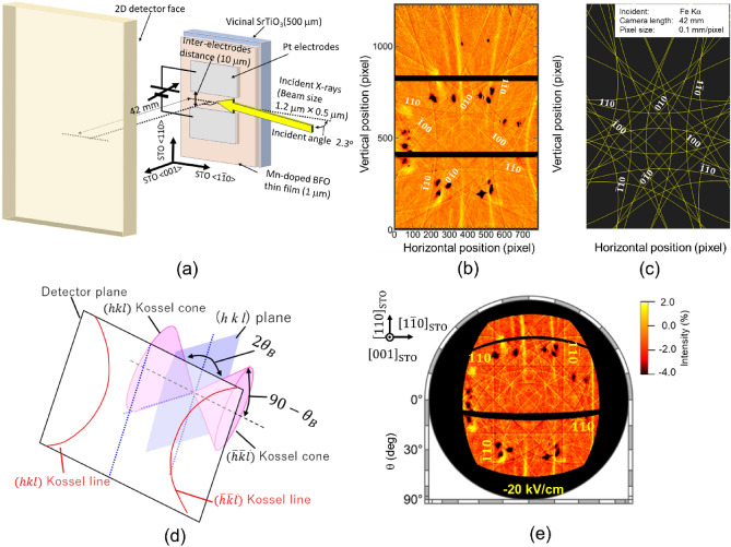
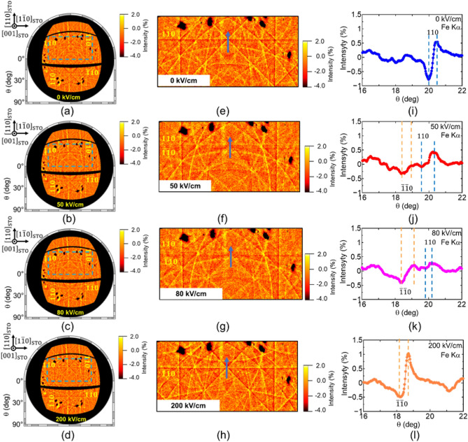
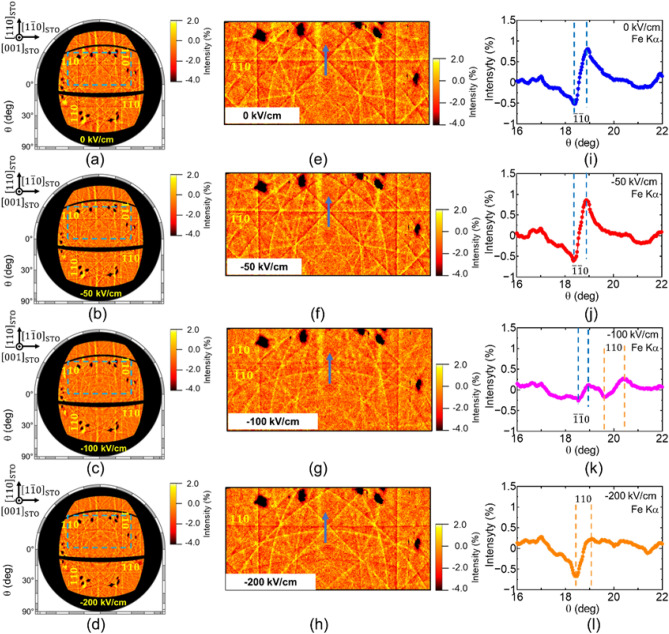
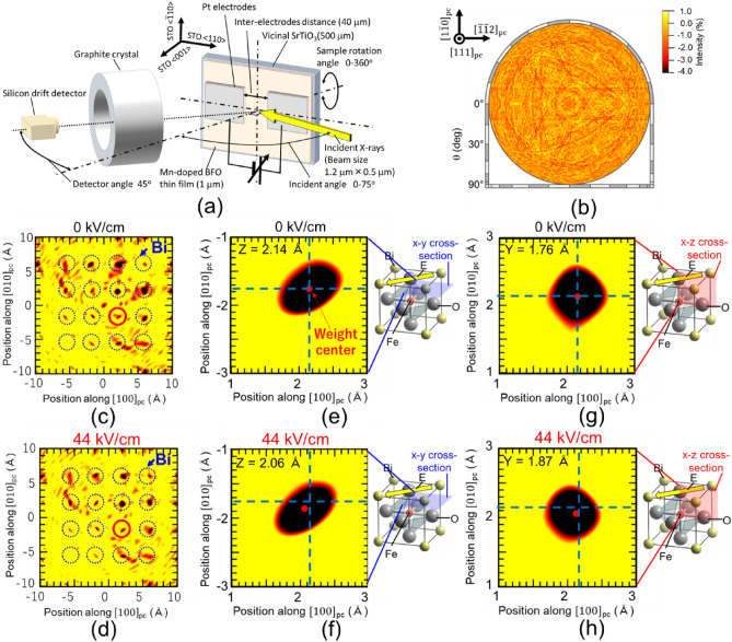
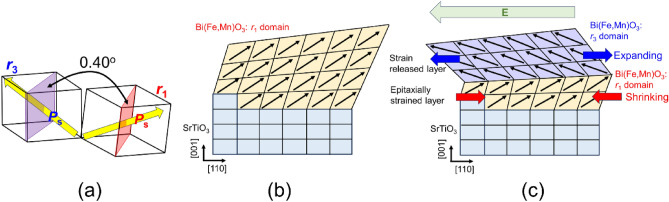
A intermediate multidomain state and large crystallographic tilting of 1.78° for the (hh0)pc planes of a (001)pc-oriented single-domain Mn-doped BiFeO3 (BFMO) thin film were found when an electric field was applied along the [110]pc direction. The anomalous crystallographic tilting was caused by ferroelastic domain switching of the 109° domain switching. In addition, ferroelastic domain switching occurred via an intermediate multidomain state. To investigate these switching dynamics under an electric field, we used in situ fluorescent X-ray induced Kossel line pattern measurements with synchrotron radiation. In addition, in situ inverse X-ray fluorescence holography (XFH) experiments revealed that atomic displacement occurred under an applied electric field. We attributed the atomic displacement to crystallographic tilting induced by a converse piezoelectric effect. Our findings provide important insights for the design of piezoelectric and ferroelectric materials and devices.


Conflict of interest statement

The authors declare no competing interests.

Figures

Figure 1
Figure 1
In situ Kossel line pattern measurements under electric field. (a) Schematic of sample structure and measurement setup. (b) Fe Kα Kossel line pattern under − 20 kV/cm applied electric field after poling by application of − 200 kV/cm electric field. (c) Calculated Kossel pattern by Fe Kα radiation. (d) Schematic of Kossel pattern detection by 2D detector. (e) Orthogonal projection along [001]pc direction of Fe Kα Kossel line pattern under − 20 kV/cm applied electric field, projected onto Ewald sphere in k-space.
Figure 2
Figure 2
Fe Kα Kossel line patterns under electric field of 0–200 kV/cm. (ad) Orthographic projection of Fe Kα Kossel line pattern projected onto Ewald sphere in k-space. (eh) Magnified images of regions indicated by blue-dashed lines in (ad), respectively. (il) Cross-sectional profiles along blue arrows in (eh), respectively, under (a, e, i) 0 kV/cm, (b, f, j) 50 kV/cm, (c, g, k) 80 kV/cm, and (d, h, l) 200 kV/cm fields. Under 50 and 80 kV/cm fields, the BFMO thin film shows an intermediate multidomain state because of anomalous domain switching.
Figure 3
Figure 3
Fe Kα Kossel line patterns under electric field of 0–200 kV/cm. (ad) Orthographic projection of Fe Kα Kossel line pattern projected onto Ewald sphere in k-space. (eh) magnified images of regions indicated by blue-dashed lines in (ad), respectively. (il) Cross-sectional profiles along blue arrows in (eh), respectively, under (a, e, i) 0 kV/cm, (b, f, j) − 50 kV/cm, (c, g, k) − 100 kV/cm, and (d, h, l) − 200 kV/cm electric fields. Under a − 100 kV/cm field, the BFMO thin film shows an intermediate multidomain state because of anomalous domain switching.
Figure 4
Figure 4
Atomic structure measurements under 0 and 44 kV/cm by in situ inverse XFH. (a) Schematic of sample structure and measurement setup for inverse XFH. (b) Orthographic projection of Fe Kα hologram pattern acquired under 0 kV/cm, projected onto Ewald sphere in k-space after symmetric operations belonging to point group 3 m, (c, d) Two-dimensional atomic images at z = 2 Å plane. (e, f) xy and (g, h) xz cross-sectional images around Bi atoms indicated by red circles in (c, d), respectively, under (c, e, g) 0 kV/cm and (d, f, h) 44 kV/cm. The red dots in (e–h) are weight centers of Bi atoms, showing displacement under electric field. For the {x, y, z} coordinate system, the xy and xz planes are defined as the [h00]pc–[0k0]pc and [h00]pc–[00 l]pc planes, respectively, and the origin of (x, y, z) = (0, 0, 0) is set at the position of the Fe atom.
Figure 5
Figure 5
Schematics of ferroelastic 109° domain switching via intermediate multidomain state. (a) schematic of pure 109° domain, (b) Single-domain BFMO thin film and (c) intermediate multidomain structure under electric field. In the 109° domain, the angle between (hh0)pc planes in the r1 and r3 domain is 0.40°. However, in an epitaxially strained single-domain BFMO film, the epitaxially strained layer cannot easily undergo ferroelastic domain switching, resulting in intermediate multidomain state.

References

    1. Eliseev EA, Morozovska AN, Svechnikov GS, Gopalan V, Shur VY. Static conductivity of charged domain walls in uniaxial ferroelectric semiconductors. Phys. Rev. B. 2011;83:235313-1-7. doi: 10.1103/PhysRevB.83.235313. - DOI
    1. Jiang AQ, Wang C, Jin KJ, Liu XB, Scott JF, Hwang CS, Tang TA, Lu HB, Yang GZ. A resistive memory in semiconducting BiFeO3 thin-film capacitors. Adv. Mater. 2011;23:1277–1281. doi: 10.1002/adma.201004317. - DOI - PubMed
    1. Tsurumaki A, Yamada H, Sawa A. Impact of Bi deficiencies on ferroelectric resistive switching characteristics observed at p-type Schottky-like Pt/Bi1–δFeO3 interfaces. Adv. Funct. Mater. 2012;22:1040–1047. doi: 10.1002/adfm.201102883. - DOI
    1. Choi T, Lee S, Choi YJ, Kiryukhin X, Cheong S-W. Switchable ferroelectric diode and photovoltaic effect in BiFeO3. Science. 2009;324:63–66. doi: 10.1126/science.1168636. - DOI - PubMed
    1. Glass AM, von der Linde D, Negran TJ. Highvoltage bulk photovoltaic effect and the photorefractive process in LiNbO3. Appl. Phys. Lett. 1974;25:233–235. doi: 10.1063/1.1655453. - DOI