Template directed perovskite X-ray detectors towards low ionic migration and low interpixel cross talking
- PMID: 38933912
- PMCID: PMC11197728
- DOI: 10.1016/j.fmre.2021.10.004
Template directed perovskite X-ray detectors towards low ionic migration and low interpixel cross talking
Abstract
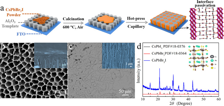
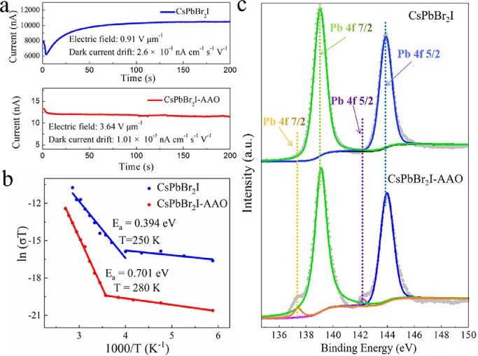
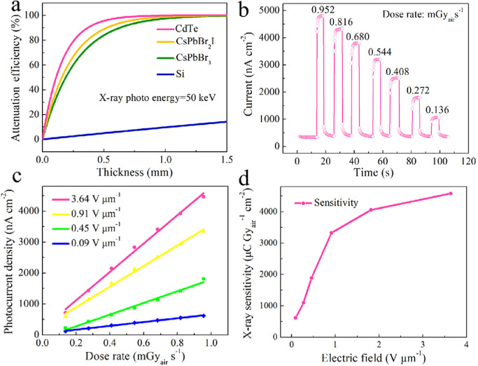
The metal halide perovskites exhibit excellent performance as the direct X-ray detectors owing to their strong absorption capability, long carrier lifetime and diffusion length, radiation ruggedness, etc. For imaging applications, the ionic migration of perovskites and charge sharing effect between the adjacent pixels have a significantly negative impact on the spatial resolution. Herein, for the first time, the porous anodic aluminum oxides (AAO) have been used as a template to grow the CsPbBr2I thick film for the direct X-ray detection. Benefiting from the oxygen passivation effect, the activation energy for ionic migration has been observed to increase to 0.701 eV, whereas the dark current drift (1.01 × 10⁻⁵ nA cm-1s-1V-1) is one to two orders of magnitude lower than the other lead halide perovskite single crystals and films. Moreover, the AAO insulating wall effectively blocks the charge diffusion effect across a pixel pitch of 10 μm. Overall, the findings reported in this study open a new route for reducing the ionic migration and pixel crosstalk, thus, bringing the perovskite X-ray detectors close to the practical applications.
Keywords: Aluminum oxides (AAO); Crosstalk; Perovskite; X-ray detection.
© 2021 The Authors. Publishing Services by Elsevier B.V. on behalf of KeAi Communications Co. Ltd.
Conflict of interest statement
The authors declare that they have no conflicts of interest in this work.
Figures


References
-
- Yaffe M.J., Rowlands J.A. X-ray detectors for digital radiography. Phys. Med. Bio. 1997;42:1. - PubMed
-
- Adachi S., Tokuda S., Ishida S. A CMOS detector readout front-end for X-ray digital radiography system. IEEE Trans. Nucl. Sci. 1996;43:249–255.
-
- Zhao W., Rowlands J.A. X-ray imaging using amorphous selenium: feasibility of a flat panel self-scanned detector for digital radiology. Medic. Phys. 1995;22:1595–1604. - PubMed
-
- Zhu M., Niu G., Tang J. Elemental Se: fundamentals and its optoelectronic applications. J. Mater. Chem. C. 2019;7:2199–2206.
-
- Szeles C., Soldner S.A., Vydrin S., et al. CdZnTe semiconductor detectors for spectroscopic x-ray imaging. IEEE Trans. Nucl. Sci. 2008;55:572–582.
LinkOut - more resources
Full Text Sources