Review
. 2024 May 10;17(13):4390-4425.
doi: 10.1039/d3ee03638c. eCollection 2024 Jul 2.

All-perovskite tandem solar cells: from fundamentals to technological progress

Affiliations
Review

All-perovskite tandem solar cells: from fundamentals to technological progress

Jaekeun Lim et al. Energy Environ Sci. .

Abstract

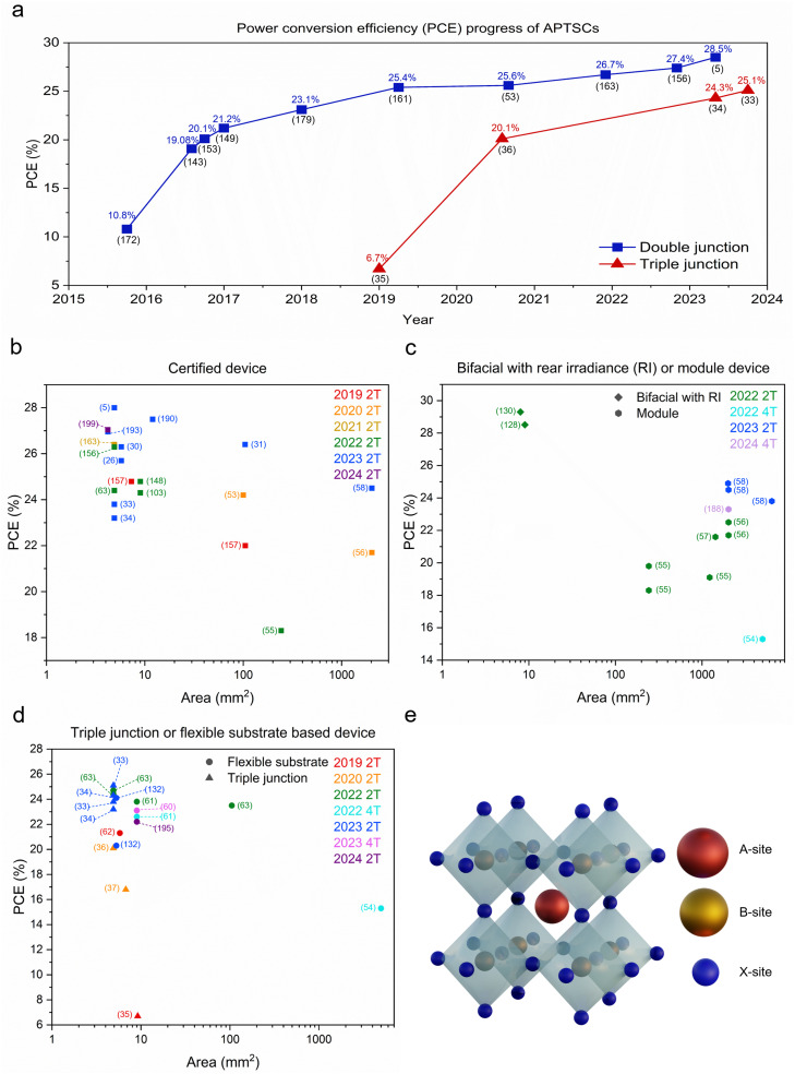
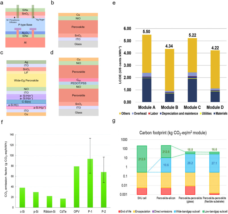
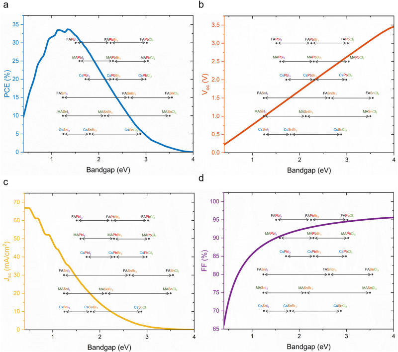
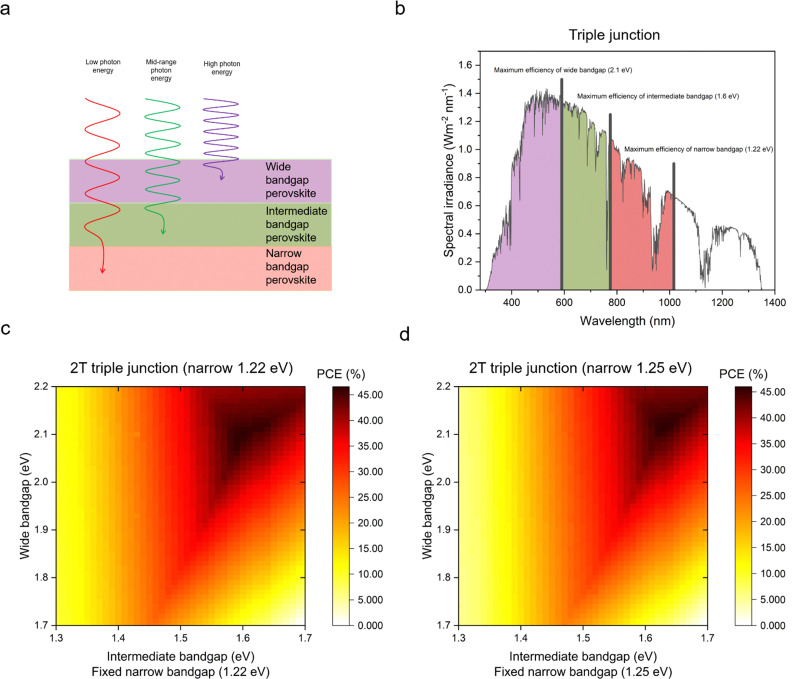
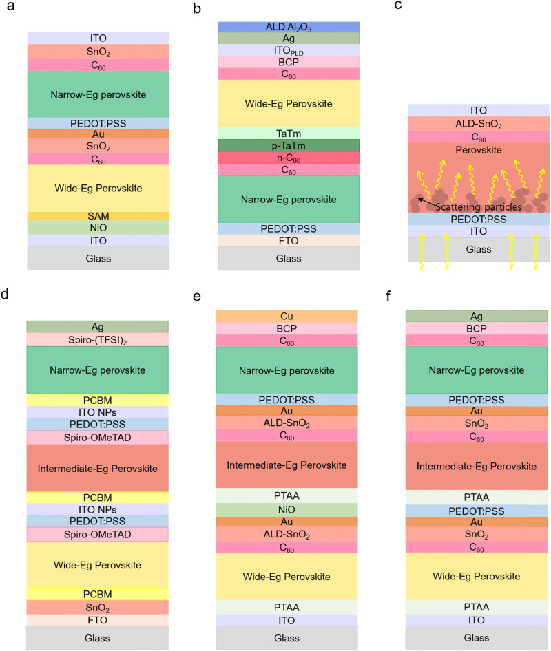
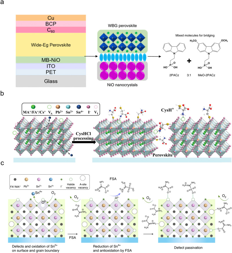
Organic-inorganic perovskite materials have gradually progressed from single-junction solar cells to tandem (double) or even multi-junction (triple-junction) solar cells as all-perovskite tandem solar cells (APTSCs). Perovskites have numerous advantages: (1) tunable optical bandgaps, (2) low-cost, e.g. via solution-processing, inexpensive precursors, and compatibility with many thin-film processing technologies, (3) scalability and lightweight, and (4) eco-friendliness related to low CO2 emission. However, APTSCs face challenges regarding stability caused by Sn2+ oxidation in narrow bandgap perovskites, low performance due to V oc deficit in the wide bandgap range, non-standardisation of charge recombination layers, and challenging thin-film deposition as each layer must be nearly perfectly homogenous. Here, we discuss the fundamentals of APTSCs and technological progress in constructing each layer of the all-perovskite stacks. Furthermore, the theoretical power conversion efficiency (PCE) limitation of APTSCs is discussed using simulations.


Conflict of interest statement

There are no conflicts to declare.

Figures

Fig. 1
Fig. 1. Summary graphs regarding efficiencies and active areas of APTSCs and the structure of perovskite. (a) This graph shows the power conversion efficiency progress of APTSCs regarding double and triple junctions with efficiency and according reference number just below (in brackets). The bifacial APTSCs are not included. (b) The scatter graph showing the efficiency (vertical axis) and area (horizontal axis) of APTSCs, regarding certified devices showing also the reference numbers. (c) The scatter graph showing the efficiency (vertical axis) and area (horizontal axis) of 2T and 4T APTSCs, containing the following information: bifacial and module device as well as the reference numbers. (d) The scatter graph showing the efficiency (vertical axis) and area (horizontal axis) of 2T and 4T APTSCs involving flexible substrate APTSC and triple junction APTSC information with the reference numbers. Device details (PCE, active area, terminal, and note) are in Table S1 (ESI†) regarding Fig. 1a–d. (e) The standard ABX3 perovskite structure.
Fig. 2
Fig. 2. Low cost and low carbon footprint APTSCs: (a) conventional multi-crystalline silicon solar module. (b) The n–i–p planar structure of a perovskite single junction module. (c) The silicon/perovskite tandem solar module. (d) The perovskite/perovskite solar module. (e) Comparison of LCOE from figure (a)–(d). © 2018. Elsevier All rights reserved. (f) The past carbon footprint of c-Si, p-Si, ribbon-Si, CdTe, organic photovoltaic (OPV), and perovskite (P1: TiO2 based perovskite module, P2: ZnO based module). © 2018. Royal Society of Chemistry All rights reserved. (g) The recent carbon footprint of a silicon heterojunction (SHJ) cell, perovskite–silicon tandem (wide-bandgap perovskite: (Cs, FA)Pb(I, Br)3), perovskite–perovskite tandem with a glass substrate and perovskite–perovskite tandem with a flexible substrate consisting of a wide-bandgap (Cs, FA, MA)Pb(I, Br)3 and narrow-bandgap (FA, MA)(Sn, Pb)I3 perovskite. © 2020. American Association for the Advancement of Science All rights reserved.
Fig. 3
Fig. 3. Prediction of single junction solar cells. (a) Shockley–Queisser limit graphs in terms of PCE, (b) Voc, (c) Jsc and (d) FF with the bandgaps of the different A-site, B-site and X-site perovskite compositions (the same colour indicates the same mono or polyatomic ions).
Fig. 4
Fig. 4. Prediction of double junction (tandem) solar cells: (a) scheme of photon energy absorption by wide and narrow bandgap perovskites in double junctions, (b) spectral irradiance graph showing theoretical maximum power conversion efficiency bandgaps for a 2-terminal (2T) double junction, (c) theoretical efficiency limit of tandem solar cells in 2T, which is a monolithic structure considering narrow bandgaps (1.1–1.6 eV) and wide bandgaps (1.6–2.2 eV), and (d) theoretical efficiency limit of tandem solar cells in 4-terminal (4T), which is a stacked structure mechanically considering narrow bandgaps (1.1–1.6 eV) and wide bandgaps (1.6–2.2 eV).
Fig. 5
Fig. 5. Prediction of triple junction (multi-junction) solar cells. (a) Scheme of photon energy absorption by wide and narrow bandgap perovskites in triple junctions, (b) spectral irradiance graph showing theoretical maximum power conversion efficiency bandgaps for a triple junction with a 1.22 eV narrow bandgap. (c) Theoretical efficiency limit of triple junction solar cells with a monolithic structure considering the narrow bandgap (the fixed value is 1.22 eV), intermediate bandgap (1.3–1.7 eV) and wide bandgap (1.7–2.2 eV), and (d) theoretical efficiency limit of triple junction solar cells in a monolithic architecture considering the narrow bandgap (a fixed value of 1.25 eV), intermediate bandgap (1.3–1.7 eV) and wide bandgap (1.7–2.2 eV).
Fig. 6
Fig. 6. Standard double junction configuration of tandem solar cells and configuration of all perovskite tandem modules. (a) 2-Terminal (2T) configuration. (b) 4-Terminal (4T) mechanically stacked, (c) and 4-terminal-optically splitting configuration. The optical splitter separates the high photon energies and low photon energies. High photon energies are absorbed by wide bandgap perovskite layers and low photon energies are absorbed by narrow bandgap perovskite layers. © 2021. John Wiley and Sons All rights reserved. (d) Scheme of 2-terminal all-perovskite-based tandem module configuration with interconnection (dead area indicated by red dashed lines) consisting of patterns 1, 2 and 3 (P1, P2 and P3) and active area (green dashed lines). (e) Scheme of 4-terminal all-perovskite-based tandem module configuration. TCO is the transparent conductive oxide. CTL is the charge transport layer. WB PVK is the wide bandgap perovskite layer. RL is the recombination layer.
Fig. 7
Fig. 7. Various types of APTSCs. (a) Scheme of the bifacial APTSC configuration. © 2022. Springer Nature All rights reserved. (b) Another type of bifacial APTSC configuration. © 2022. American Chemical Society All rights reserved. (c) Illustration of the scattering particles (resin) functioning with increasing photon path length in the narrow bandgap perovskite film. © 2022. American Association for the Advancement of Science All rights reserved. (d) The APTSC structure of a fully solution-processed triple junction. (e) (f) Other types of solution-processed triple junction APTSC configurations. © 2020. American Chemical Society All rights reserved. © 2020. Springer Nature All rights reserved.
Fig. 8
Fig. 8. Interfacial type of perovskite film treatment. (a) Bridge structure formed using mixed molecules of 2PACz and MeO-2PACz between a wide bandgap perovskite and a NiO nanocrystal layer. © 2022. Springer Nature All rights reserved. (b) Illustration of the crystal growth process employing CysHCl in the Sn–Pb perovskite. © 2023. John Wiley and Sons All rights reserved. (c) Illustration of antioxidation using formamidine sulfinic acid (FSA) in the Sn–Pb perovskite. © 2020. Springer Nature All rights reserved.
Fig. 9
Fig. 9. Several configurations of charge recombination layers. (a) Device configuration including the charge recombination layer of spiro-MeOTAD/PEDOT:PSS/PEI (polyethylenimine)/PCBM:PEI. © 2020. Royal Society of Chemistry. All rights reserved. (b) Cell structure including the charge recombination layer of Spiro-MeOTAD/PEDOT:PSS/C60. © 2017. American Chemical Society All rights reserved. (c) Device structure including an organic dopant (F6-TCNNQ) in TaTm for the charge recombination layer configuration. © 2016. John Wiley and Sons. All rights reserved. (d) Device configuration including the charge recombination layer of (fluoride silane and polyethylenimine ethoxylated (PEIE) in trichloro(3,3,3-trifluoropropyl)silane) FPTS/C60/BCP/Cu:Au alloy/PEDOT:PSS. © 2018. John Wiley and Sons. All rights reserved. (e) Device structure before simplifying the charge recombination layer of C60/SnO2−x/ITO/PTAA. (f) Device structure after simplifying the charge recombination layer of C60/SnO2−x. © 2020. Springer Nature. All rights reserved.
None
Jaekeun Lim
None
Nam-Gyu Park
None
Sang Il Seok
None
Michael Saliba

Similar articles

Cited by

References

    1. Park J. Kim J. Yun H.-S. Paik M. J. Noh E. Mun H. J. Kim M. G. Shin T. J. Il Seok S. Nature. 2023;616:724–730. doi: 10.1038/s41586-023-05825-y. - DOI - PubMed
    1. Best Research-Cell Efficiency Chart | Photovoltaic Research | NREL, https://www.nrel.gov/pv/cell-efficiency.html, (accessed 11 January 2024)
    1. Todorov T. Gershon T. Gunawan O. Sturdevant C. Guha S. Appl. Phys. Lett. 2014;105(17):173902. doi: 10.1063/1.4899275. - DOI
    1. Liu S. Lu Y. Yu C. Li J. Luo R. Guo R. Liang H. Jia X. Guo X. Wang Y.-D. Zhou Q. Wang X. Yang S. Sui M. Müller-Buschbaum P. Hou Y. Nature. 2024;628:306–312. doi: 10.1038/s41586-024-07226-1. - DOI - PubMed
    1. Lin R. Wang Y. Lu Q. Tang B. Li J. Gao H. Gao Y. Li H. Ding C. Wen J. Wu P. Liu C. Zhao S. Xiao K. Liu Z. Ma C. Deng Y. Li L. Fan F. Tan H. Nature. 2023;620:994–1000. doi: 10.1038/s41586-023-06278-z. - DOI - PubMed

LinkOut - more resources