. 2024 Jul 4;15(1):5615.
doi: 10.1038/s41467-024-49841-6.

Topological Fermi-arc surface state covered by floating electrons on a two-dimensional electride

Affiliations

Topological Fermi-arc surface state covered by floating electrons on a two-dimensional electride

Chan-Young Lim et al. Nat Commun. .

Abstract

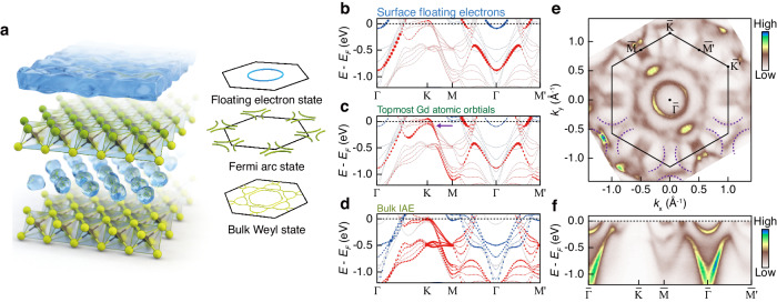
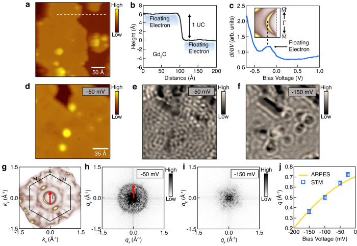
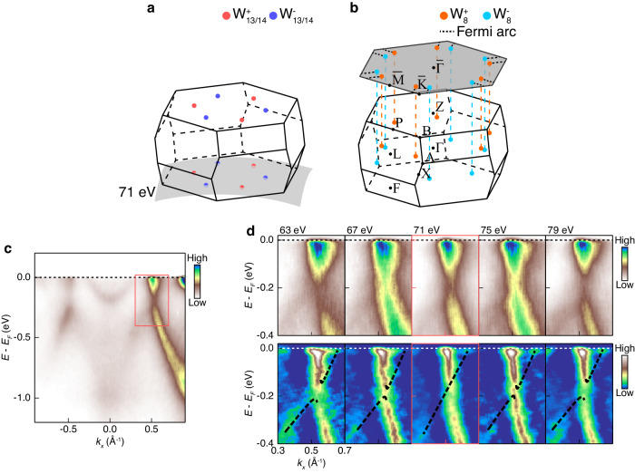
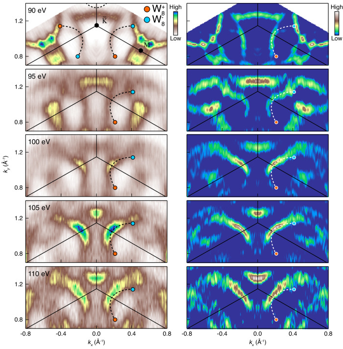
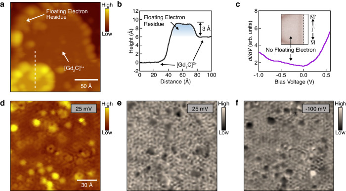
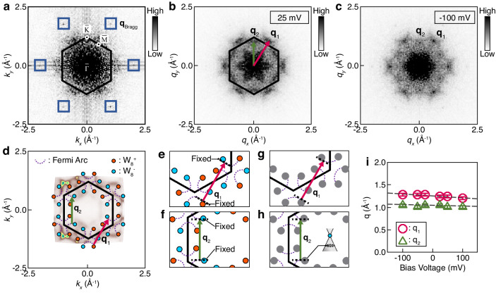
Two-dimensional electrides can acquire topologically non-trivial phases due to intriguing interplay between the cationic atomic layers and anionic electron layers. However, experimental evidence of topological surface states has yet to be verified. Here, via angle-resolved photoemission spectroscopy (ARPES) and scanning tunnelling microscopy (STM), we probe the magnetic Weyl states of the ferromagnetic electride [Gd2C]2+·2e-. In particular, the presence of Weyl cones and Fermi-arc states is demonstrated through photon energy-dependent ARPES measurements, agreeing with theoretical band structure calculations. Notably, the STM measurements reveal that the Fermi-arc states exist underneath a floating quantum electron liquid on the top Gd layer, forming double-stacked surface states in a heterostructure. Our work thus not only unveils the non-trivial topology of the [Gd2C]2+·2e- electride but also realizes a surface heterostructure that can host phenomena distinct from the bulk.


Conflict of interest statement

The authors declare no competing interests.

Figures

Fig. 1
Fig. 1. Crystal structure and electronic structure of [Gd2C]2+·2e.
a Schematic of the crystal (left panel) and electronic (right panel) structures. In the left panel, the green and black spheres represent Gd and C atoms, respectively, forming [Gd2C]2+ layers. Blue blobs between the [Gd2C]2+ layers denote bulk interstitial anionic electrons (IAEs). The floating electrons are depicted atop the crystal structure. The right panel illustrates the electronic structure corresponding to the crystal structure. The bulk of the crystal exhibits a non-trivial band topology, hosting the bulk Weyl state. The Fermi-arc state is observed on the [Gd2C]2+ surface, while the floating electron state reveals a circular Fermi surface. bd Calculated electronic structures with contributions from electrons at the surface floating electrons (b), the topmost Gd atoms (c), and the bulk IAEs (d). Blue and red colors denote major and minor spin components, respectively. The purple arrow in (c) marks the predicted Fermi-arc dispersion. e, f Fermi surface (e) and high-symmetric line dispersions (f) obtained from ARPES measurements with 90 eV photons. The Fermi surface was symmetrized along Γ¯K¯ direction. The black solid line on (e) represents the 1st Brillouin zone (BZ) boundary, and the purple dashed lines near K¯ and K¯ points guide the expected Fermi arcs.
Fig. 2
Fig. 2. STM measurements on floating electrons of [Gd2C]2+·2e.
a Topographic image of as-cleaved [Gd2C]2+·2e sample. Vbias = −100 mV and It = 100 pA. b Height profile obtained along the dashed line in (a). There is one unit cell (UC) height difference between the neighboring terraces. c dI/dV spectrum measured on the terrace of (a). The peak around −0.25 V indicates the onset of the band of floating electrons. The inset shows the band of floating electrons measured by ARPES. d Enlarged topographic image. Vbias = −50 mV and It = 100 pA. e dI/dV map at Vbias = −50 mV. The quasiparticle interference (QPI) patterns are observed. Lock-in modulation amplitude (Vmod) of 10 mV is used. f dI/dV map at Vbias = −150 mV. Vmod = 10 mV. g Fermi surface measured by ARPES. The red arrow indicates the nesting vector of the band of floating electrons. h Fourier transformed the image of (e). The QPI modulation vector (q) corresponds to the nesting vector in (g), which is marked by the same-sized red arrow. i Fourier transformed image of (f). j Dispersion of q by the bias voltage. The error bar represents the momentum uncertainty resulting from the resolution of dI/dV maps.
Fig. 3
Fig. 3. ARPES measurements on Weyl cones in [Gd2C]2+·2e.
a, b Schematic 3D BZs of [Gd2C]2+·2e displaying W13/14 (a) and W8 Weyl points (WPs) (b). Spheres with different colors in (a, b) represent WPs with opposite chirality. The gray surfaces a, b denote 71 eV ARPES measurement plane and the (111) surface-projected BZ, respectively. On the surface-projected BZ, WPs are connected to other WPs with opposite chirality at neighboring BZs via Fermi arcs drawn with black dashed line segments. c 71 eV Γ¯M¯ dispersion with Weyl state inside the red box indicating expected Weyl cone position. d Weyl state measured with various photon energies near 71 eV. The upper panels are raw images, and the lower panels are their 2D curvature plots to enhance band features. Black dashed lines in the lower panels serve as guides for eyes to visualize the Weyl cones.
Fig. 4
Fig. 4. ARPES measurements on Fermi arcs in [Gd2C]2+·2e.
Photon energy-dependent Fermi surfaces (FSs) near the K¯ point (left) and their 2D curvature plots to enhance FS features (right). Both panels are symmetrized with respect to kx = 0 for better visualization of Fermi arcs. Light red and light blue points indicate W8+ and W8 WPs, respectively. Black solid lines denote BZ boundaries. Fermi arcs are drawn with dashed line segments connecting W8 WPs. In the original data for the 90 eV Fermi surface, all Fermi arcs are displayed, but they are omitted in the other plots except one used for comparison.
Fig. 5
Fig. 5. STM measurements on Fermi-arc states of [Gd2C]2+·2e.
a Topographic image of [Gd2C]2+ surface, where the floating electrons are removed by heating the sample at 80 K for 1 h. Vbias = −100 mV and It = 100 pA. b Height profile taken along the dashed line in (a). c dI/dV spectrum measured on the [Gd2C]2+ surface. The band onset of the floating electrons is missing in the dI/dV spectrum, which is further confirmed in the ARPES data (inset). d Enlarged topographic image of [Gd2C]2+ surface. Vbias = 25 mV and It = 100 pA. e dI/dV map at Vbias = 25 mV. Vmod = 10 mV. f dI/dV map at Vbias = −100 mV. Vmod = 10 mV.
Fig. 6
Fig. 6. STM analysis on Fermi-arc states of [Gd2C]2+·2e.
a Fourier transformed the image of the topographic image (Fig. 5d). The blue boxes indicate the Bragg peaks. b, c Fourier transformed images of the dI/dV maps (Fig. 5e, f). Two distinct QPI modulation vectors are identified as q1 (red arrow) and q2 (green arrow). d Schematics illustrating Fermi-arc states, overlaid with ARPES data for clarity. The q1 and q2 vectors joining the Fermi-arc states are assigned by considering their sizes and directions. e, f Nesting conditions for the q1 and q2 vectors. g, h Nesting conditions for q1 and q2 at a lowered bias voltage. The dispersion of Fermi-arc states is minimal near the Weyl cone, leading the q1 and q2 vectors to remain unaltered significantly. i Dispersion of q1 (red circles) and q2 (green triangles) by the bias voltage. The dashed lines are given for eye-guides. The error bar represents the momentum uncertainty resulting from the resolution of dI/dV maps.

References

    1. Huang H, Jin K-H, Zhang S, Liu F. Topological electride Y2C. Nano Lett. 2018;18:1972–1977. doi: 10.1021/acs.nanolett.7b05386. - DOI - PubMed
    1. Hirayama M, Matsuishi S, Hosono H, Murakami S. Electrides as a new platform of topological materials. Phys. Rev. X. 2018;8:031067.
    1. Liu S, et al. Ferromagnetic Weyl fermions in two-dimensional layered electride Gd2C. Phys. Rev. Lett. 2020;125:187203. doi: 10.1103/PhysRevLett.125.187203. - DOI - PubMed
    1. Zhao S, Li Z, Yang J. Obtaining two-dimensional electron gas in free space without resorting to electron doping: an electride based design. J. Am. Chem. Soc. 2014;136:13313–13318. doi: 10.1021/ja5065125. - DOI - PubMed
    1. Guan S, Yang SA, Zhu L, Hu J, Yao Y. Electronic dielectric and plasmonic properties of two-dimensional electride materials X2N (X=Ca, Sr): A first-principles study. Sci. Rep. 2015;5:12285. doi: 10.1038/srep12285. - DOI - PMC - PubMed