. 2024 Jul 5;15(1):5651.
doi: 10.1038/s41467-024-49576-4.

Surface photogalvanic effect in Ag2Te

Affiliations

Surface photogalvanic effect in Ag2Te

Xiaoyi Xie et al. Nat Commun. .

Abstract

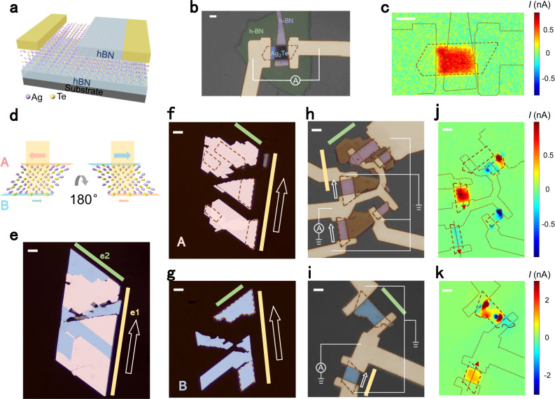
The bulk photovoltaic effect (BPVE) in non-centrosymmetric materials has attracted significant attention in recent years due to its potential to surpass the Shockley-Queisser limit. Although these materials are strictly constrained by symmetry, progress has been made in artificially reducing symmetry to stimulate BPVE in wider systems. However, the complexity of these techniques has hindered their practical implementation. In this study, we demonstrate a large intrinsic photocurrent response in centrosymmetric topological insulator Ag2Te, attributed to the surface photogalvanic effect (SPGE), which is induced by symmetry reduction of the surface. Through diverse spatially-resolved measurements on specially designed devices, we directly observe that SPGE in Ag2Te arises from the difference between two opposite photocurrent flows generated from the top and bottom surfaces. Acting as an efficient SPGE material, Ag2Te demonstrates robust performance across a wide spectral range from visible to mid-infrared, making it promising for applications in solar cells and mid-infrared detectors. More importantly, SPGE generated on low-symmetric surfaces can potentially be found in various systems, thereby inspiring a broader range of choices for photovoltaic materials.


Conflict of interest statement

The authors declare no competing interests.

Figures

Fig. 1
Fig. 1. Crystal structure and photocurrent response of Ag2Te.
a, b Unit cell of Ag2Te in three-dimensional perspective (a) and the projection of (100) plane (b). The inky blue axis, the orange-pink plane, and the black dot indicate the screw rotation axis C2b, the glide mirror plane Mb~ and the center of inversion symmetry, respectively. The colorized axes show the unit cell vectors. The dashed black axes in a show the laboratory coordinates, where the nanoplate surface (1¯01) is parallel to the x-y plane. b Schematic of the microscopic symmetry operations. The blue-outlined polyhedron transforms to the dotted blue one after the operation of a pure rotation and then coincides with the yellow one after a glide of 1/2b along the b-axis. The red-outlined polyhedron transforms to the dotted red one after the operation of a pure mirror and then coincides with the yellow one after a glide of 1/2c along the c-axis. c Main: power dependence of the photocurrent response in Ag2Te. The red points are the measured data and the black solid line is the fitting curve of IP1.1, respectively. Inset: false-color optical image of the device with the scheme of the short-circuit photocurrent measurement. d Mapping of the photocurrent response of the device. The laser wavelength in c, d is 690 nm and the power in d is ~70 μW. The scale bars are all 5 μm.
Fig. 2
Fig. 2. Crystallographic orientation and linear polarization dependence of the photocurrent response in Ag2Te.
a False-color optical image of an Ag2Te nanoplate etched into 5 samples (s1-s5). The white dotted rhomboid outlines the initial Ag2Te nanoplate. The yellow and green bars mark the two edges of the nanoplate, e1 and e2. b Photocurrent mapping measured with a wiring scheme depicted in a of the device. The laser wavelength is 690 nm and the power is ~100 μW. The scale bars in a, b are all 10 μm. c Line-profile of the photocurrent extracted from (b) along the red arrows marked in (b). The red arrows also indicate the photocurrent flow directions. The orange-pink shaded areas in c represent the electrode regions. d Simulated polarization dependence of Ib (photocurrent perpendicular to b-axis) and Ib (photocurrent along b-axis).ex and ey are the light polarization unit vectors. e Polarization dependence measured at the center of s2 marked by the green dot in a under the illumination of 690 nm and 1310 nm. The fitting curve of 690 nm is a constant corresponding to βyyy = βyxx. The fitting curve of 1310 nm is I = 9.40 + 2.76cos(2(φ−0.109°)), where φ is the polarization angle, corresponding to βyxx = 0.546βyyy. The polarization dependence of s3 was also measured at its center marked by the red dot in a, but the signal always remains equal to zero. Light blue coordinates in a mark the directions of the polar coordinates. f, g Schematics of the bulk photovoltaic effect (BPVE) (f) and the surface photogalvanic effect (SPGE) (g). In BPVE, a unidirectional photocurrent is generated in the bulk of non-centrosymmetric materials under illumination. In SPGE, photocurrent flows are generated on the top and bottom surfaces, allowed by specific surface symmetry, and often produce a net photocurrent due to the bulk absorption.
Fig. 3
Fig. 3. Evidence for the surface origin of the photocurrent response in Ag2Te.
ac, Schematic structure of the hBN(hexagonal born nitride)-Ag2Te-hBN device (a), its false-color optical image with scheme of the measurement (b), and photocurrent response mapping (c). Outlines of Ag2Te, electrodes, and top-hBN have been marked with dotted lines. dk, The turn-over experiment of Ag2Te. d Schematic of the turn-over process. The pink and blue arrows represent the opposite responses generated from surfaces A and B, respectively. The direction of the total response is determined by the upper surface, which would be reversed if the sample is turned over. eg False-color optical images of the sample. One Ag2Te nanoplate on polydimethylsiloxane (PDMS) (e) was mechanically cut into fragments and parts of them (recolored as blue) were lifted up and consequently turned over to B side up (g) by another PDMS. The rest parts (recolored as pink) keep A side up (f) the same as the initial nanoplate shown in (e). hk, False-color optical images and photocurrent mapping results of the two devices fabricated from (f) and (g), respectively. The red dashed lines in fk outlines the samples through the fabrication procedures. The yellow and green bars in e–i mark the two edges of the nanoplate, e1 and e2. White arrows in ei indicate the same crystallographic direction along e1. Red arrows in j, k indicate the photocurrent directions. The laser wavelength is 690 nm and the power is ~80 μW in c, j, k. The scale bars are all 5 μm.
Fig. 4
Fig. 4. Performance of the surface photogalvanic effect in Ag2Te.
a Thickness dependence of the responsivity of Ag2Te. Measurements of all the samples are carried out under the same 690-nm illumination with a power of ~80μW. The data is fitted by R=R01expαd, where R0 is the responsivity of an individual surface, d is the thickness of Ag2Te and α is the transmission coefficient. b Measured BPV coefficients of non-centrosymmetric materials (WS2 nanotube, 2H-MoS2 with strain gradient (sg), strained 3R-MoS2, CuInP2S6 (CIPS) (2D and 3D), BaTiO3 (BTO), BiFeO3 (BFO), (BDA)(EA)2Pb3Br10, Fe-doped LiNbO3 (LNO:Fe), twisted double bilayer graphene (TDBG), TaAs) and equivalent PV coefficient of Ag2Te. Data of (BDA)(EA)2Pb3Br10 and TDBG are taken from their responsivity, data of LNO:Fe is β333, and others are effective values of β.

References

    1. Sturman, B. & Fridkin, V. The Photovoltaic and Photorefractive Effects in Noncentrosymmetric Materials Vol. 1 (Routledge, 1992).
    1. Koch WTH, Munser R, Ruppel W, Würfel P. Anomalous photovoltage in BaTiO3. Ferroelectrics. 1976;13:305–307. doi: 10.1080/00150197608236596. - DOI
    1. Glass AM, D. von der L, Negran TJ. High-voltage bulk photovoltaic effect and the photorefractive process in LiNbO3. Appl. Phys. Lett. 1974;25:233–235. doi: 10.1063/1.1655453. - DOI
    1. Spanier JE, et al. Power conversion efficiency exceeding the Shockley–Queisser limit in a ferroelectric insulator. Nat. Photonics. 2016;10:611–616. doi: 10.1038/nphoton.2016.143. - DOI
    1. Yang SY, et al. Above-bandgap voltages from ferroelectric photovoltaic devices. Nat. Nanotechnol. 2010;5:143–147. doi: 10.1038/nnano.2009.451. - DOI - PubMed

LinkOut - more resources