

Stable chalcogenide Ge-Sb-Te heterostructures with minimal Ge segregation
- PMID: 38977811
- PMCID: PMC11231325
- DOI: 10.1038/s41598-024-66441-y
Stable chalcogenide Ge-Sb-Te heterostructures with minimal Ge segregation
Abstract
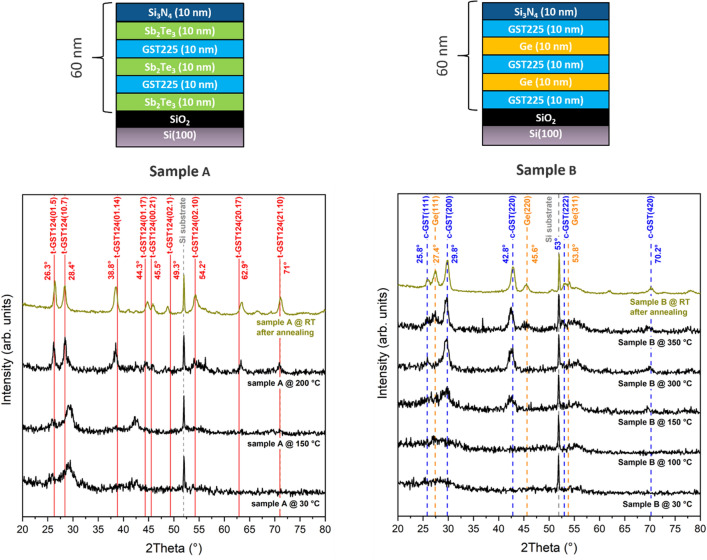
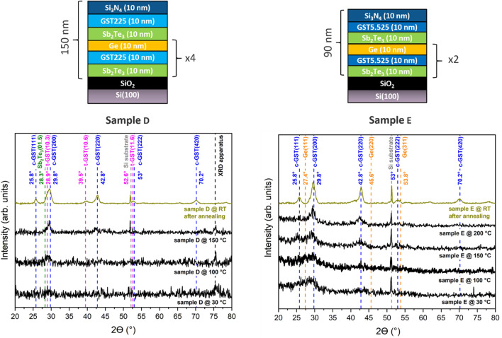
Matching of various chalcogenide films shows the advantage of delivering multilayer heterostructures whose physical properties can be tuned with respect to the ones of the constituent single films. In this work, (Ge-Sb-Te)-based heterostructures were deposited by radio frequency sputtering on Si(100) substrates and annealed up to 400 °C. The as-deposited and annealed samples were studied by means of X-ray fluorescence, X-ray diffraction, scanning transmission electron microscopy, electron energy loss spectroscopy and Raman spectroscopy. The heterostructures, combining thermally stable thin layers (i. e. Ge-rich Ge5.5Sb2Te5, Ge) and films exhibiting fast switching dynamics (i. e. Sb2Te3), show, on the one side, higher crystallization-onset temperatures than the standard Ge2Sb2Te5 alloy and, on the other side, none to minimal Ge-segregation.
Keywords: Crystallization; GST; Ge; Ge segregation; Ge-rich; PCM; Sb2Te3; Sputtering.
© 2024. The Author(s).
Conflict of interest statement
The authors declare no competing interests.
Figures


References
-
- Fizza K, et al. QoE in IoT: A vision, survey and future directions. Discov. Internet Things. 2021;1(1):4. doi: 10.1007/s43926-021-00006-7. - DOI
-
- Yan A, et al. Thin-film transistors for integrated circuits: Fundamentals and recent progress. Adv. Funct. Mater. 2024;34(3):2304409. doi: 10.1002/adfm.202304409. - DOI
-
- Calvi S, et al. Highly sensitive organic phototransistor for flexible optical detector arrays. Org. Electron. 2022;102:106452. doi: 10.1016/j.orgel.2022.106452. - DOI
-
- Rapisarda, M. et al. Water stable organic thin film transistors (TFTs) made on flexible substrates. In 2015 IEEE 15th International Conference on Nanotechnology (IEEE-NANO). 1430–1433. 10.1109/NANO.2015.7388907 (IEEE, 2015).
-
- Rapisarda M. et al. Fully-organic flexible tactile sensor for advanced robotic applications. In 2014 IEEE 9th Nanotechnology Materials and Devices Conference (NMDC), Aci Castello (CT), Italy. 45–48 10.1109/NMDC.2014.6997418 (IEEE, 2014).
LinkOut - more resources
Full Text Sources
Research Materials
