. 2024 Jul 24;24(29):9042-9049.
doi: 10.1021/acs.nanolett.4c02231. Epub 2024 Jul 15.

Functionality Expansion of Guided Mode Radiation via On-Chip Metasurfaces

Affiliations

Functionality Expansion of Guided Mode Radiation via On-Chip Metasurfaces

Lin Deng et al. Nano Lett. .

Abstract

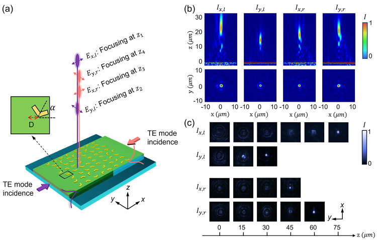
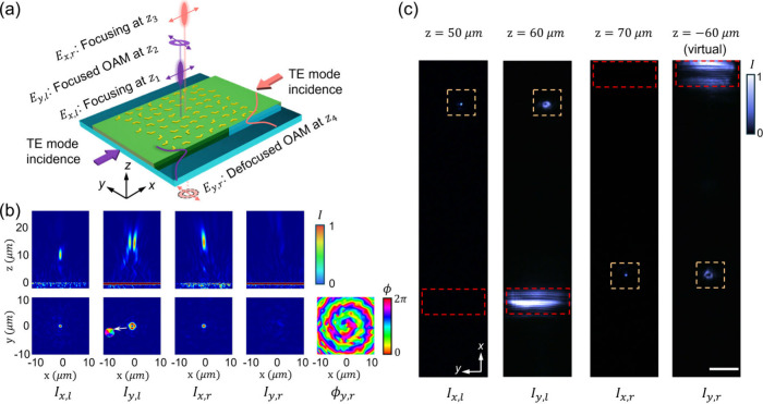
On-chip metasurfaces play a crucial role in bridging the guided mode and free-space light, enabling full control over the wavefront of scattered free-space light in an optimally compact manner. Recently, researchers have introduced various methods and on-chip metasurfaces to engineer the radiation of guided modes, but the total functions that a single metasurface can achieve are still relatively limited. In this work, we propose a novel on-chip metasurface design that can multiplex up to four distinct functions. We can efficiently control the polarization state, phase, angular momentum, and beam profile of the radiated waves by tailoring the geometry of V-shaped nanoantennas integrated on a slab waveguide. We demonstrate several innovative on-chip metasurfaces for switchable focusing/defocusing and for multifunctional generators of orbital angular momentum beams. Our on-chip metasurface design is expected to advance modern integrated photonics, offering applications in optical data storage, optical interconnection, augmented reality, and virtual reality.

Keywords: integrated photonics; multiplexing; on-chip metasurface; vortex beam.


Conflict of interest statement

The authors declare no competing financial interest.

Figures

Figure 1
Figure 1
(a) Illustration of realizing the focusing and defocusing functions with a two-port waveguide. (b) Phase evolution of the scattered light from V-shaped nanoantennas under the excitation of evanescent waves with TE polarization. (c) Symmetry consideration for V-shaped nanoantennas subject to incidence from opposite directions. (d) E-field distributions for the on-chip metasurface that generates focused and defocused beams when the waveguide mode is incident from the left and right side. The top and bottom panels show the electric field intensity of Ex in the plane of z = 13 μm and y = 0 μm, respectively. (e) Phase distributions of the generated focused beam and defocused beam in the plane of y = 0 μm.
Figure 2
Figure 2
(a) Schematic of the optical setup to measure the on-chip metasurface. The insets show the SEM images of the fabricated device with different magnifications. The scale bars are 10 μm and 250 nm, respectively. HWP: Half wave plate. LP: Linear polarizer. CCD: Charge-coupled device. (b) Experimental demonstration of focusing and defocusing effects. The images on the two sides show the intensity distribution when light is coupled to the waveguide from the left and right gratings (scale bar: 10 μm). The images in the middle show the zoom-in intensity distribution of out-coupled light with polarization orthogonal to the incident light, when the focal plane of the objective lens varies from −40 to 40 μm with respect to the metasurface plane in 10 μm increments (scale bar: 50 μm). The areas of the metasurface and the grating coupler are denoted by yellow and red boxes, respectively. (c) Intensity map in the xz plane cutting through the center of the metasurface. (d) Intensity distribution across the focal point along the x- and y-axis when light is incident from the left side.
Figure 3
Figure 3
(a) Illustration of realizing four focal points for the scattered Ex and Ey components with left- and right-incidence of the fundamental TE waveguide mode. The inset shows a V-shaped nanoantenna with rotation and dislocation. (b) Simulated intensity profiles of the Ex,l, Ey,l, Ex,r, and Ey,r components with the focal distance of 24, 15, 18, and 21 μm. The top row shows the focusing effect in the xz plane, while the bottom row displays the intensity distribution in the xy plane at the target focusing distance. (c) Measured beam evolution along the z-axis at different positions. The designed focal distances are set at 75, 30, 45, and 60 μm.
Figure 4
Figure 4
(a) Illustration of realizing focused OAM beams, defocused OAM beams, and two focused beams for four combinations of detection polarization and incident direction. (b) Simulated intensity for Ex,l, Ey,l, Ex,r, and Ey,r components with the focal distance z = 10, 15, 15, and −15 μm, respectively. The top row shows the focusing and defocusing effect in the xz plane, while the bottom row displays the intensity distribution in the xy plane at the distance z = 10, 15, 15, and 15 μm, respectively. ϕy,r shows the simulated phase distribution of the OAM beam at z = 15 μm. (c) Measured beam profile along the z-axis at certain positions. The designed focal distances for the fabricated device are set at z = 50, 60, 70, and −60 μm for Ex,l, Ey,l, Ex,r an,d Ey,r components of the scattered light (scale bar: 50 μm). The areas of the metasurface and the grating coupler are denoted by yellow and red boxes, respectively.

References

    1. Hsiao H. H.; Chu C. H.; Tsai D. P. Fundamentals and applications of metasurfaces. Small Methods 2017, 1 (4), 1600064.10.1002/smtd.201770041. - DOI
    1. Xiong B.; Deng L.; Peng R.; Liu Y. Controlling the degrees of freedom in metasurface designs for multi-functional optical devices. Nanoscale Advances 2019, 1 (10), 3786–3806. 10.1039/C9NA00343F. - DOI - PMC - PubMed
    1. Jahani S.; Jacob Z. All-dielectric metamaterials. Nature Nanotechnol. 2016, 11 (1), 23–36. 10.1038/nnano.2015.304. - DOI - PubMed
    1. Yu N.; Capasso F. Flat optics with designer metasurfaces. Nature materials 2014, 13 (2), 139–150. 10.1038/nmat3839. - DOI - PubMed
    1. Kildishev A. V.; Boltasseva A.; Shalaev V. M. Planar photonics with metasurfaces. Science 2013, 339 (6125), 1232009.10.1126/science.1232009. - DOI - PubMed

LinkOut - more resources