. 2024 Jul 17;15(1):6001.
doi: 10.1038/s41467-024-50329-6.

Realization of a two-dimensional Weyl semimetal and topological Fermi strings

Affiliations

Realization of a two-dimensional Weyl semimetal and topological Fermi strings

Qiangsheng Lu et al. Nat Commun. .

Abstract

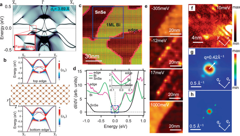
A two-dimensional (2D) Weyl semimetal, akin to a spinful variant of graphene, represents a topological matter characterized by Weyl fermion-like quasiparticles in low dimensions. The spinful linear band structure in two dimensions gives rise to distinctive topological properties, accompanied by the emergence of Fermi string edge states. We report the experimental realization of a 2D Weyl semimetal, bismuthene monolayer grown on SnS(Se) substrates. Using spin and angle-resolved photoemission and scanning tunneling spectroscopies, we directly observe spin-polarized Weyl cones, Weyl nodes, and Fermi strings, providing consistent evidence of their inherent topological characteristics. Our work opens the door for the experimental study of Weyl fermions in low-dimensional materials.


Conflict of interest statement

The authors declare no competing interests.

Figures

Fig. 1
Fig. 1. Topology, lattice property, and band structure of 2D Weyl semimetal, α-bismuthene grown on SnS.
a Overview of Dirac/Weyl semimetals and their topological boundary states. b Side and top views of the lattice structure of bismuthene and SnS substrate. The red dashed squares indicate the unit cell of bismuthene and SnS. c Large-scale STM image of bismuthene grown on SnS substrate. d The height profile is taken along the red arrow in (c). e Zoom-in STM images of bismuthene (top) and the surface of SnS (bottom). The red dashed squares indicate the unit cell of SnS and bismuthene. f Calculated band structure of free-standing bismuthene. g Calculated band structure of bismuthene on SnSe.
Fig. 2
Fig. 2. ARPES and first-principles band structure of Weyl fermion states in epitaxial bismuthene.
a ARPES Fermi surface taken from bismuthene on SnSe. b ARPES spectra of bismuthene taken along the line of “cut1” marked in (a). c Overlay of calculated band structure on the ARPES spectrum along “cut1''. The magenta lines are bands along the direction of Γ¯-X¯1 while the green lines are bands in the direction perpendicular to Γ¯-X¯2. d Calculated band spectra with the inclusion of photoemission matrix elements. eg Same as b–d but for bands of bismuthene on SnSe along the line of “cut2'', which passes across the Weyl node. h Second derivative of the ARPES spectrum in the red box in (e). i Energy distribution curves (EDC) from the ARPES spectrum inside the red box in (e). The blue dotted lines mark the maximum of each EDC. The red solid line plots the EDC taken at the momentum of the Weyl point. j–l Same as b–d, but for bands of bismuthene on SnS along “cut2''.
Fig. 3
Fig. 3. Spin texture of 2D Weyl fermion states.
a ARPES spectrum along “cut1” marked in Fig. 2a. b Calculated band structure along “cut1” with the inclusion of photoemission matrix elements. The bands are colored according to the calculated expectation value 〈sy〉 of each state. c Spin-resolved momentum distribution curves (MDC) taken at E = −0.1 eV along the line marked by the pink dashed arrows in (a) and (b). The blue and red curves are the photoelectron intensity recorded in the “spin-down” and “spin-up” channels of the spin detector, respectively. d The spin polarization extracted from the MDCs in (c). The shaded area indicates net spin polarization of 〈sy〉. The formula for error bars can be found in the Supplementary Information. e ARPES spectrum along “cut2” marked in Fig. 2a. f 2D spin-resolved ARPES map of 〈sy〉 taken along “cut2''. The blue and red dots represent the photoelectron signals recorded in the “spin-down” and “spin-up” channels of the spin detector, respectively. g Calculated electron band structure along “cut2'', which is colored according to the expectation value 〈sy〉 of each state. h Spin-resolved MDCs of 〈sy〉 taken at E = −0.25 eV along the line marked by the green dashed arrows in (e) and (g). i Spin polarization of 〈sy〉 extracted from the MDCs in (h). j–l Same as g–i, but for the spin component 〈sx〉. m In-plane spin texture of iso-energy contours at E = −0.25 eV. The red and blue circles schematically depict the iso-energy contours of two valleys at E = −0.25 eV. The black arrows indicate the in-plane spin orientation of the Weyl fermion states.
Fig. 4
Fig. 4. Bulk–boundary correspondence in 2D Weyl semimetals.
a The edge bands and projected bulk bands of a semi-infinite bismuthene film on SnSe with an open boundary in the (010) direction. The bands are weighted with the charge density near the edge. d0 = 3.89 Å is the relaxed interlayer spacing between bismuthene and SnSe substrate. b The connection of Fermi string edge bands to bulk Weyl nodes. The band structure was calculated by using a tight-binding model in which sz is conserved. c STM topography of bismuthene on SnSe. d Differential conductivity dI/dV spectra with the bias voltage aligned with the energy of Weyl nodes. The green curve is the averaged spectrum taken at the green grid inside the bismuthene patches shown in (c). The black curve is the averaged spectrum from the black grid on the surface of SnSe. The magenta curve is the averaged spectrum from the magenta points at the edges of the bismuthene patches. The inset shows the zoom-in dI/dV curves around the energy of Weyl nodes. e dI/dV map over the area marked by the blue box in c at bias voltage V= −305, −12, 17, and 1000 meV. f High-resolution dI/dV map at bias voltage V = +10 meV. g The corresponding Fourier transform of the dI/dV map in f, showing the quasiparticle interference (QPI) pattern. h The calculated quasiparticle interference pattern with spin-dependent scattering probability is considered.

References

    1. Wan X, Turner AM, Vishwanath A, Savrasov SY. Topological semimetal and fermi-arc surface states in the electronic structure of pyrochlore iridates. Phys. Rev. B. 2011;83:205101. doi: 10.1103/PhysRevB.83.205101. - DOI
    1. Xu S-Y, et al. Discovery of a weyl fermion semimetal and topological fermi arcs. Science. 2015;349:613–617. doi: 10.1126/science.aaa9297. - DOI - PubMed
    1. Lv BQ, et al. Experimental discovery of weyl semimetal TaAs. Phys. Rev. X. 2015;5:031013.
    1. Soluyanov AA, et al. Type-II Weyl semimetals. Nature. 2015;527:495–8. doi: 10.1038/nature15768. - DOI - PubMed
    1. Armitage NP, Mele EJ, Vishwanath A. Weyl and Dirac semimetals in three-dimensional solids. Rev. Mod. Phys. 2018;90:015001. doi: 10.1103/RevModPhys.90.015001. - DOI

LinkOut - more resources