. 2024 Jul 19;15(1):6109.
doi: 10.1038/s41467-024-50330-z.

Evidence of a distinct collective mode in Kagome superconductors

Affiliations

Evidence of a distinct collective mode in Kagome superconductors

Bin Hu et al. Nat Commun. .

Abstract

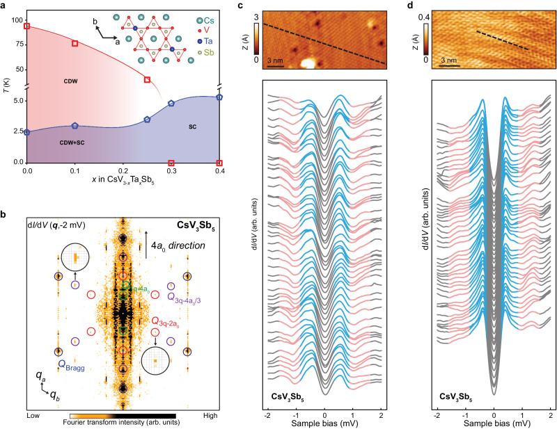
The collective modes of the superconducting order parameter fluctuation can provide key insights into the nature of the superconductor. Recently, a family of superconductors has emerged in non-magnetic kagome materials AV3Sb5 (A = K, Rb, Cs), exhibiting fertile emergent phenomenology. However, the collective behaviors of Cooper pairs have not been studied. Here, we report a distinct collective mode in CsV3-xTaxSb5 using scanning tunneling microscope/spectroscopy. The spectral line-shape is well-described by one isotropic and one anisotropic superconducting gap, and a bosonic mode due to electron-mode coupling. With increasing x, the two gaps move closer in energy, merge into two isotropic gaps of equal amplitude, and then increase synchronously. The mode energy decreases monotonically to well below 2 Δ and survives even after the charge density wave order is suppressed. We propose the interpretation of this collective mode as Leggett mode between different superconducting components or the Bardasis-Schrieffer mode due to a subleading superconducting component.


Conflict of interest statement

The authors declare no competing interests.

Figures

Fig. 1
Fig. 1. Observation of bosonic mode in CsV3Sb5.
a Phase diagram of CsV3-xTaxSb5. The superconducting (SC) transition temperature increases while the charge density wave (CDW) transition temperature decreases with increasing x. The CDW is undetectable when x > 0.30. The transition temperatures of SC and CDW are obtained from transport measurement. The inset of (a) shows the crystal structure of CsV3Sb5. b The Fourier transform of the tunneling conductance dI/dV map taken at –2mV on a typical as-cleaved Sb surface of CsV3Sb5, showing the 4a0 CDW, 2a0×2a0 CDW, 4a0/3×4a0/3 CDW and 4a0/3×4a0/3 pair density wave (PDW), and intriguing quasi-particle interference patterns, respectively. The a0 in (b) is the lattice constant. The Q1q-4a0, (Q3q-4a0/3) and QBragg in (b) are the wave vectors of 4a0 CDW, 4a0/3 CDW/PDW, and Bragg peaks, which are indicated by the colored circles. c A series of dI/dV spectra (lower panel) obtained along the line-cut (black dotted line) on the topography in the upper panel, showing two SC gaps accompanied by a pair of peak-dip-hump features just outside the SC gaps, indicative of a bosonic mode. d Same as in (c) but over a line-cut in a different spatial region (upper panel), where the dI/dV spectra (lower panel) are dominated by the spectral line-shape of a smaller gap in a more subtle two-gap structure. The peak-dip-hump features outside of the SC gaps are also clearly visible indicating the presence of a bosonic mode. For (c, d), the scanning tunneling microscope (STM) scanning parameters are bias setup (Vs) = −600 mV, current setup (It) = 400 pA and Vs = –20 mV, It = 1 nA, respectively, and the scanning tunneling spectroscopy (STS) parameters are the same: Vs = –2.0 mV, It = 1 nA, and lockin modulation amplitude (Vmod) = 0.05 mV.
Fig. 2
Fig. 2. Analysis of the SC gaps and bosonic mode energy in pristine CsV3Sb5.
a Two types of representative dI/dV spectra. The bigger and smaller SC gaps corresponding to the peak-to-peak distances are labeled by Δb and Δs, respectively. b The corresponding derivative spectra d2I/dV2 of (a), where the energies of the SC gaps and the bosonic mode offset by the two gaps can be quantitatively extracted. Labels in (b) are defined as Es,b±=±(Δs,b+Ω), where Ω is the energy of bosonic mode. c Histograms of Δs, Δb, Es, and Eb, plotted with the same counts of bins and fitted by normal distributions. The averaged values are Δs = 0.40(0.09) meV, Δb = 0.62(0.09) meV, Es = 1.16(0.09) meV, and Eb=1.42(0.09) meV, where the error is based on the energy resolution. The extracted bosonic mode energy is 0.76(0.13) meV from Es and Δs, and 0.80(0.13) meV from Eb and Δb. d A series of dI/dV spectra obtained on the Cs and Sb surfaces of CsV3Sb5 in different regions obtained under the tunneling conditions Vs = –2.0 mV, Vmod = 0.1 mV, It = 1 nA. The spatially-averaged spectrum is highlighted by the red solid line. e The derivative of the spatially-averaged dI/dV curve, from which the energies of the bosonic mode offset by the SC gaps (E+ peak and E dip in d2I/dV2) can be determined (Ω¯ = 0.76 meV, Δ¯ = 0.40 meV). f Two-gap Dynes functions description of the spatially-averaged dI/dV spectrum isolated from (d), showing good overall agreement. The difference between the two-gap Dynes functions and the experimental data demarcates the contribution due to the bosonic mode, which is marked by the shadowed region with cyan color. The two gap functions are shown as polar plots in the inset of (f).
Fig. 3
Fig. 3. Analysis of superconducting gaps and the bosonic mode in Ta-dopped CsV3Sb5 (CsV3-xTaxSb5, x = 0.10, 0.25 and 0.40).
STM images obtained on the Sb surface of CsV2.90Ta0.10Sb5 (a), CsV2.75Ta0.25Sb5 (b), and CsV2.60Ta0.40Sb5 (c), respectively (Vs = –100 mV, It = 1 nA). The corresponding Fourier transform (inset) shows the disappearing of 2a0×2a0 CDW with increasing of x. A series of dI/dV spectra obtained in different region on the Cs and Sb surface of CsV2.90Ta0.10Sb5 (d), CsV2.75Ta0.25Sb5 (e), and CsV2.60Ta0.40Sb5 (f) under the tunneling conditions Vs = –2 mV, Vmod = 0.05 mV, It = 1 nA, where the spatially-averaged spectra are highlighted in each stack plot by orange, green and sky-blue colors, respectively. Two-gap Dynes functions description of the spatially-averaged dI/dV spectra of CsV2.90Ta0.10Sb5 (g), CsV2.75Ta0.25Sb5 (h), and CsV2.60Ta0.40Sb5 (i), respectively. The experimental data (black circles) matches very well with the two-gap Dynes functions curves (colored solid lines). The features of bosonic modes manifest in their difference just outside the SC gaps marked by the shadowed region with cyan color. The two gap functions are shown as polar plots in the insets of (g–i). The red circles and blue circles in (ac) represent the wave vectors of 2a0×2a0 CDW and Bragg peaks, respectively.
Fig. 4
Fig. 4. The evolution of SC gaps and the collective mode energy in CsV3-xTaxSb5.
a Plot of Δ1,min, Δ1,max and Δ2 (marked in the inset) determined from the spatially-averaged spectrum as a function of the Ta-substitution ratio x. Δ1,min and Δ1,max are the minima and maxima SC amplitude of the SC gap 1, and Δ2 is the SC amplitude of the SC gap 2. b The gap to Tc ratio, 2Δ2/kBTc and 2Δ1,max/kBTc, as a function of Ta-substitution x, showing that 2Δ2/kBTc is large and indicative of a strong-coupling superconductor in the undoped case, decreases and approaches to the BCS value (3.53) with increasing x, while 2Δ1,max/kBTc is always close to BCS value for all x. kB is the Boltzmann constant. c Scatter plot of the bosonic mode energy Ω versus Ta-substitution ratio x, showing that Ω decreases with increasing x. d Plot of Ω/2Δ versus Ta-substitution ratio x, showing Ω is far below the pair-breaking energy 2Δ at large x, where Δ is the SC gap measured by the coherence peak-to-peak distance. In pristine CsV3Sb5, Δ is effectively determined by the smaller SC gap. e Schematics of the Higgs-Leggett mode, showing the amplitude and phase fluctuation of the SC order parameters. The Higgs mode is marked by black arrows. The Leggett mode (ϕ1–ϕ2) is marked by the wavy line and colored arrows, where ϕ1 and ϕ2 are the SC phase. f Plot of transition temperature Tc as a function of mode energy Ω. The data are taken or extracted from the STM works on kagome superconductors reported here, NbSe2, twisted bilayer graphene, twisted trilayer graphene, Pr0.88LaCe0.12CuO4, one-unit-cell FeSe, EuRbFe4As4, Ba0.6K0.4Fe0.2As,, and Na(Fe0.975Co0.025)As, as well as from the Uemura plot. The Tcs of twisted trilayer graphene are extracted from ref. . The dashed line in (f) indicates the Uemura line (kBTc ∼ Ω/4). The error bars in (c, d) are based on the energy resolution statistical deviation.

References

    1. Jandke, J., Hlobil, P., Schackert, M., Wulfhekel, W. & Schmalian, J. Coupling to real and virtual phonons in tunneling spectroscopy of superconductors. Phys. Rev. B93, 060505 (2016).10.1103/PhysRevB.93.060505 - DOI
    1. Lee, J. et al. Interplay of electron-lattice interactions and superconductivity in Bi2Sr2CaCu2O8+δ. Nature442, 546–550 (2006). 10.1038/nature04973 - DOI - PubMed
    1. Niestemski, F. C. et al. A distinct bosonic mode in an electron-doped high-transition-temperature superconductor. Nature450, 1058–1061 (2007). 10.1038/nature06430 - DOI - PubMed
    1. Liu, C. et al. Detection of bosonic mode as a signature of magnetic excitation in one-unit-cell FeSe on SrTiO3. Nano Lett19, 3464–3472 (2019). 10.1021/acs.nanolett.9b00144 - DOI - PubMed
    1. Uemura, Y. J. Dynamic superconductivity responses in photoexcited optical conductivity and Nernst effect. Phys. Rev. Mater.3, 104801 (2019).10.1103/PhysRevMaterials.3.104801 - DOI

LinkOut - more resources