. 2024 Aug 7;24(31):9711-9719.
doi: 10.1021/acs.nanolett.4c02519. Epub 2024 Jul 25.

Spatially Resolved Quantum Sensing with High-Density Bubble-Printed Nanodiamonds

Affiliations

Spatially Resolved Quantum Sensing with High-Density Bubble-Printed Nanodiamonds

Brian W Blankenship et al. Nano Lett. .

Abstract

Nitrogen-vacancy (NV-) centers in nanodiamonds have emerged as a versatile platform for a wide range of applications, including bioimaging, photonics, and quantum sensing. However, the widespread adoption of nanodiamonds in practical applications has been hindered by the challenges associated with patterning them into high-resolution features with sufficient throughput. In this work, we overcome these limitations by introducing a direct laser-writing bubble printing technique that enables the precise fabrication of two-dimensional nanodiamond patterns. The printed nanodiamonds exhibit a high packing density and strong photoluminescence emission, as well as robust optically detected magnetic resonance (ODMR) signals. We further harness the spatially resolved ODMR of the nanodiamond patterns to demonstrate the mapping of two-dimensional temperature gradients using high frame rate widefield lock-in fluorescence imaging. This capability paves the way for integrating nanodiamond-based quantum sensors into practical devices and systems, opening new possibilities for applications involving high-resolution thermal imaging and biosensing.

Keywords: Bubble Printing; Magnetic Resonance Imaging; NV centers; Nanodiamonds; Quantum Sensing; Thermometry.


Conflict of interest statement

The authors declare no competing financial interest.

Figures

Figure 1
Figure 1
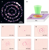
Bubble printing of nanodiamonds. (A) Diagram depicting the bubble printing process. (B) Fluorescence image of a section of the painting, The Creation of Adam printed with 100 nm nanodiamonds. (C) Darkfield images of a double hexagonal structure using 35 nm NDs. (D) Corresponding fluorescence images. (E) PL spectra associated with the highlighted regions indicating the high background contrast ratio.
Figure 2
Figure 2
SEM images of printed nanodiamond structures. (A) SEM images of 35 nm double walled hexagon structure that is also shown in Figure 1D. (B) SEM images of The Creation of Adam that is also shown in Figure 1E. (C, D) Closeup images depicts the nanodiamond-substrate interface where the edge of the bubble deposited particles. Individual nanodiamonds are discernible and form closely packed beds. Loose agglomerations of particles are largely distributed close to written sections.
Figure 3
Figure 3
PL and ODMR characterizations. (A) Comparisons of PL emission spectra from sections of 100 and 35 nm nanodiamond (ND) sections of bubble printed (BP) tracks. (B) Normalized PL intensity of sections of bubble printed 100 nm diamond relative to drop casted diamond. (C) Normalized PL intensity of sections of bubble printed 35 nm diamond relative to drop casted diamond their respective ODMR curves from sampling using 32 mW of 532 nm excitation with 3 ms sampling intervals per point. (D) ODMR signal from of sections of bubble printed 100 nm diamond relative to drop casted diamond and (E) ODMR signal from sampling bubble printed sections and drop casted sections using 16 mW of 532 nm excitation with 3 ms sampling intervals per point.
Figure 4
Figure 4
Lock-In ODMR imaging experiments. (A) Nanodiamond tracks were printed into concentric circles spanning length scales relevant for laser heating. (B) These circles are used to spatially monitor the temperature across the surface of the AuNI substrate as it is irradiated by a CW 532 nm laser. (C–H) Widefield lock-in ODMR images taken at (C) 2810 MHz, (D) 2825 MHz, (E) 2845 MHz, (F) 2865 MHz, (G) 2875 MHz, and (H) 2895 MHz.
Figure 5
Figure 5
ZFS and temperature mapping. (A) A map of fitted ZFS position for the first two rings of the bullseye structure. Black pixels represent areas where there was not sufficient signal to fit a curve corresponding to areas with low concentrations of nanodiamonds. (B) ODMR data from a pixel in the central spot fitted with a bigaussian function used to calculate the ZFS. (C) Simulated temperature distribution under laser heating. (D) Calculated temperature from the ZFS map as a function of distance from the center of the laser spot as compared to the temperature simulation.

References

    1. Gulka M.; Wirtitsch D.; Ivády V.; Vodnik J.; Hruby J.; Magchiels G.; Bourgeois E.; Gali A.; Trupke M.; Nesladek M. Room-Temperature Control and Electrical Readout of Individual Nitrogen-Vacancy Nuclear Spins. Nat. Commun. 2021, 12 (1), 4421.10.1038/s41467-021-24494-x. - DOI - PMC - PubMed
    1. Hanson R.; Dobrovitski V. V.; Feiguin A. E.; Gywat O.; Awschalom D. D. Coherent Dynamics of a Single Spin Interacting with an Adjustable Spin Bath. Science 2008, 320 (5874), 352–355. 10.1126/science.1155400. - DOI - PubMed
    1. Nemoto K.; Trupke M.; Devitt S. J.; Stephens A. M.; Scharfenberger B.; Buczak K.; Nöbauer T.; Everitt M. S.; Schmiedmayer J.; Munro W. J. Photonic Architecture for Scalable Quantum Information Processing in Diamond. Phys. Rev. X 2014, 4 (3), 031022.10.1103/PhysRevX.4.031022. - DOI
    1. Abobeih M. H.; Randall J.; Bradley C. E.; Bartling H. P.; Bakker M. A.; Degen M. J.; Markham M.; Twitchen D. J.; Taminiau T. H. Atomic-Scale Imaging of a 27-Nuclear-Spin Cluster Using a Quantum Sensor. Nature 2019, 576 (7787), 411–415. 10.1038/s41586-019-1834-7. - DOI - PubMed
    1. Barclay P. E.; Fu K.-M. C.; Santori C.; Beausoleil R. G. Chip-Based Microcavities Coupled to Nitrogen-Vacancy Centers in Single Crystal Diamond. Appl. Phys. Lett. 2009, 95 (19), 191115.10.1063/1.3262948. - DOI