. 2022 Nov 28;10(4):nwac273.
doi: 10.1093/nsr/nwac273. eCollection 2023 Apr.

Two-dimensional superconducting MoSi2N4(MoN)4n homologous compounds

Affiliations

Two-dimensional superconducting MoSi2N4(MoN)4n homologous compounds

Zhibo Liu et al. Natl Sci Rev. .

Abstract

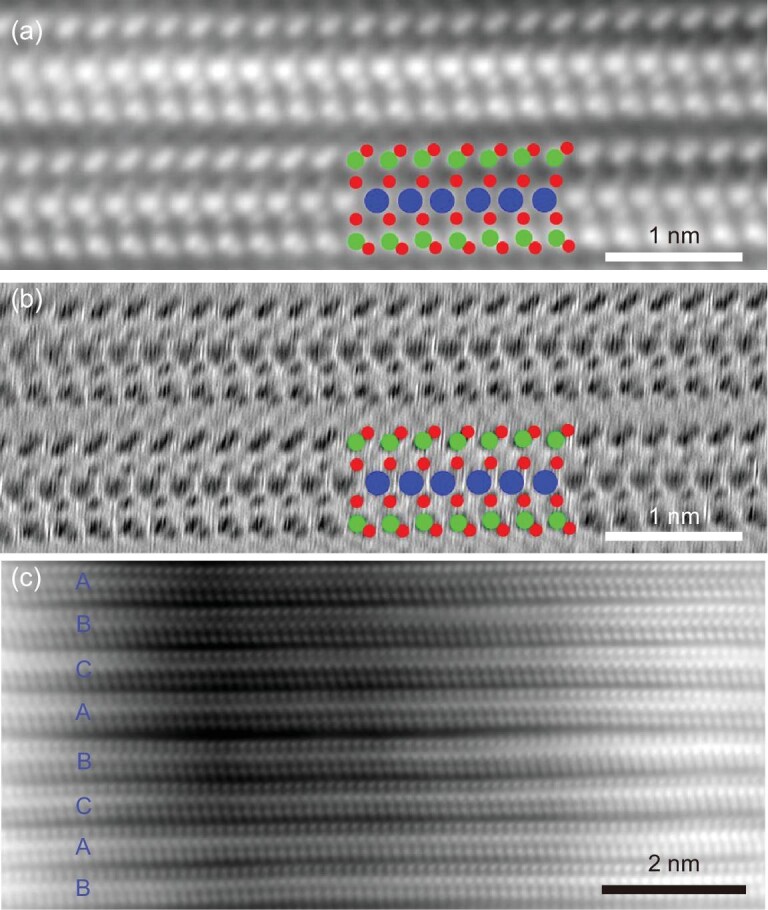
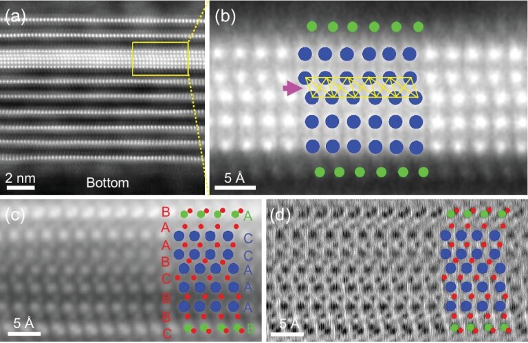
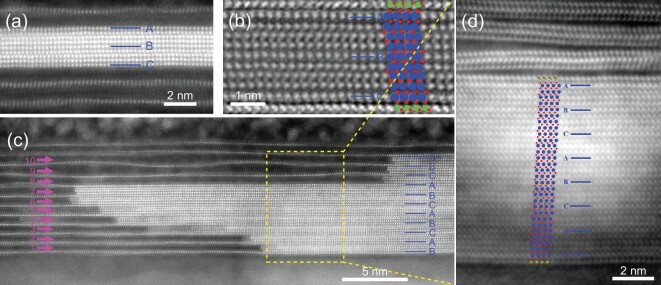
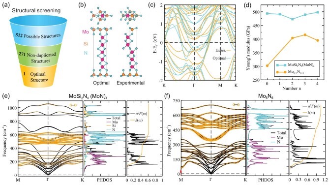
The number and stacking order of layers are two important degrees of freedom that can modulate the properties of 2D van der Waals (vdW) materials. However, the layers' structures are essentially limited to the known layered 3D vdW materials. Recently, a new 2D vdW material, MoSi2N4, without known 3D counterparts, was synthesized by passivating the surface dangling bonds of non-layered 2D molybdenum nitride with elemental silicon, whose monolayer can be viewed as a monolayer MoN (-N-Mo-N-) sandwiched between two Si-N layers. This unique sandwich structure endows the MoSi2N4 monolayer with many fascinating properties and intriguing applications, and the surface-passivating growth method creates the possibility of tuning the layer's structure of 2D vdW materials. Here we synthesized a series of MoSi2N4(MoN)4n structures confined in the matrix of multilayer MoSi2N4. These super-thick monolayers are the homologous compounds of MoSi2N4, which can be viewed as multilayer MoN (Mo4n+1N4n+2) sandwiched between two Si-N layers. First-principles calculations show that MoSi2N4(MoN)4 monolayers have much higher Young's modulus than MoN, which is attributed to the strong Si-N bonds on the surface. Importantly, different from the semiconducting nature of the MoSi2N4 monolayer, the MoSi2N4(MoN)4 monolayer is identified as a superconductor with a transition temperature of 9.02 K. The discovery of MoSi2N4(MoN)4n structures not only expands the family of 2D materials but also brings a new degree of freedom to tailor the structure of 2D vdW materials, which may lead to unexpected novel properties and applications.

Keywords: 2D layered materials; MoSi2N4; homologous compounds; iDPC-STEM; superconductivity.


Conflict of interest statement

None declared.

Figures

Figure 1.
Figure 1.
The atomic structure of multilayer MoSi2N4. (a and b) iDPC (a) and the corresponding dDPC (b) images of bilayer MoSi2N4, clearly showing the atomic sites of Mo (blue balls), Si (green balls) and N (red balls). (c) iDPC image of a rhombohedral-structured multilayer MoSi2N4 with ABC-typed stacking order.
Figure 2.
Figure 2.
The atomic structure of MoSi2N4(MoN)4. (a and b) HAADF-STEM image of MoSi2N4(MoN)4 confined in multilayer MoSi2N4 (a) and the zoomed-in view of the MoSi2N4(MoN)4 (b). (c and d) iDPC (c) and dDPC (d) images of MoSi2N4(MoN)4. The blue, green and red balls represent the Mo, Si and N atoms, respectively.
Figure 3.
Figure 3.
The atomic structure of super-thick MoSi2N4(MoN)4n. (a and b) HAADF-STEM image of MoSi2N4(MoN)8 confined in multilayer MoSi2N4 (a) and iDPC image of MoSi2N4(MoN)8 (b). The A, B and C lines indicate the Mo atomic layers aligned with the MoSi2N4 matrix. (c and d) HAADF-STEM image of one end of the MoSi2N4(MoN)4n confined in 11-layer MoSi2N4 (c) and iDPC image of MoSi2N4(MoN)28 (d). The blue, green and red balls represent the Mo, Si and N atoms, respectively.
Figure 4.
Figure 4.
Calculated structures and properties of MoSi2N4(MoN)n. (a) Diagram illustrating the process of structure screening of MoSi2N4(MoN)4. (b and c) The atomic models (b) and electronic band structures (c) of the energetically favorable structure and experimental structure of MoSi2N4(MoN)4. (d) Young's modulus of MoSi2N4(MoN)n and Mon+1Nn+2 for n = 0−4. The Young's modulus of Mo2N3 was not given due to its mechanical instability. (e and f) Phonon dispersions, vibrational PHDOS, Eliashberg function and accumulated EPC constants of MoSi2N4(MoN)4 (e) and Mo5N6 (f), where the circles in phonon dispersion plots represent the phonon linewidth γqν, related to the contribution to α2F(ω) at each q and each mode ν.

Similar articles

References

    1. Novoselov KS, Geim AK, Morozov SVet al. Electric field effect in atomically thin carbon films. Science 2004; 306: 666–9. 10.1126/science.1102896 - DOI - PubMed
    1. Zhang Y, Tan Y-W, Stormer HLet al. Experimental observation of the quantum Hall effect and Berry's phase in graphene. Nature 2005; 438: 201–4. 10.1038/nature04235 - DOI - PubMed
    1. Novoselov KS, Jiang Z, Zhang Yet al. Room-temperature quantum hall effect in graphene. Science 2007; 315: 1379. 10.1126/science.1137201 - DOI - PubMed
    1. Novoselov KS, Geim AK, Morozov SVet al. Two-dimensional gas of massless Dirac fermions in graphene. Nature 2005; 438: 197–200. 10.1038/nature04233 - DOI - PubMed
    1. Geim AK, Novoselov KS. The rise of graphene. Nat Mater 2007; 6: 183–91. 10.1038/nmat1849 - DOI - PubMed

LinkOut - more resources