

Impact of surface charge density modulation on ion transport in heterogeneous nanochannels
- PMID: 39117730
- PMCID: PMC11310325
- DOI: 10.1038/s41598-024-69335-1
Impact of surface charge density modulation on ion transport in heterogeneous nanochannels
Abstract
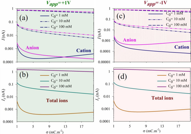
The PNP nanotransistor, consisting of emitter, base, and collector regions, exhibits distinct behavior based on surface charge densities and various electrolyte concentrations. In this study, we investigated the impact of surface charge density on ion transport behavior within PNP nanotransistors at different electrolyte concentrations and applied voltages. We employed a finite-element method to obtain steady-state solutions for the Poisson-Nernst-Planck and Navier-Stokes equations. The ions form a depletion region, influencing the ionic current, and we analyze the influence of surface charge density on the depth of this depletion region. Our findings demonstrate that an increase in surface charge density results in a deeper depletion zone, leading to a reduction in ionic current. However, at very low electrolyte concentrations, an optimal surface charge density causes the ion current to reach its lowest value, subsequently increasing with further increments in surface charge density. As such, at and , the ionic current increases by 25% when the surface charge density rises from 5 to 20 , whereas at , the ionic current decreases by 65% with the same increase in surface charge density. This study provides valuable insights into the behavior of PNP nanotransistors and their potential applications in nanoelectronic devices.
Keywords: Bipolar smart nanochannel; Depletion zone; Electroosmotic flow; PNP nanotransistor; Surface charge density.
© 2024. The Author(s).
Conflict of interest statement
The authors declare no competing interests.
Figures


Similar articles
-
Smart nanochannels: tailoring ion transport properties through variation in nanochannel geometry.Phys Chem Chem Phys. 2023 Oct 11;25(39):26716-26736. doi: 10.1039/d3cp03768a. Phys Chem Chem Phys. 2023. PMID: 37779455
-
Ionic selectivity of single nanochannels.Nano Lett. 2008 Jul;8(7):1978-85. doi: 10.1021/nl800949k. Epub 2008 Jun 18. Nano Lett. 2008. PMID: 18558784
-
Ion Transport in Multi-Nanochannels Regulated by pH and Ion Concentration.Anal Chem. 2024 Apr 9;96(14):5648-5657. doi: 10.1021/acs.analchem.4c00406. Epub 2024 Apr 1. Anal Chem. 2024. PMID: 38556994
-
Ion Transport in Intelligent Nanochannels: A Comparative Analysis of the Role of Electric Field.Anal Chem. 2023 Dec 12;95(49):18188-18198. doi: 10.1021/acs.analchem.3c03809. Epub 2023 Nov 29. Anal Chem. 2023. PMID: 38019778
-
Theoretical simulation of the ion current rectification (ICR) in nano-pores based on the Poisson-Nernst-Planck (PNP) model.Phys Chem Chem Phys. 2014 Jan 7;16(1):23-32. doi: 10.1039/c3cp51712h. Phys Chem Chem Phys. 2014. PMID: 24253284 Review.
References
-
- Liu, Z., Wang, L., Liu, Q. & Liu, G. Effect of surface charge gradient on the concentration difference driven energy conversion in nanochannel. Electrochim. Acta444, 141999. 10.1016/j.electacta.2023.141999 (2023).10.1016/j.electacta.2023.141999 - DOI
Grants and funding
LinkOut - more resources
Full Text Sources
Research Materials
Miscellaneous
