Review
. 2024 Aug 9;16(1):264.
doi: 10.1007/s40820-024-01461-x.

Performance Limits and Advancements in Single 2D Transition Metal Dichalcogenide Transistor

Affiliations
Review

Performance Limits and Advancements in Single 2D Transition Metal Dichalcogenide Transistor

Jing Chen et al. Nanomicro Lett. .

Abstract

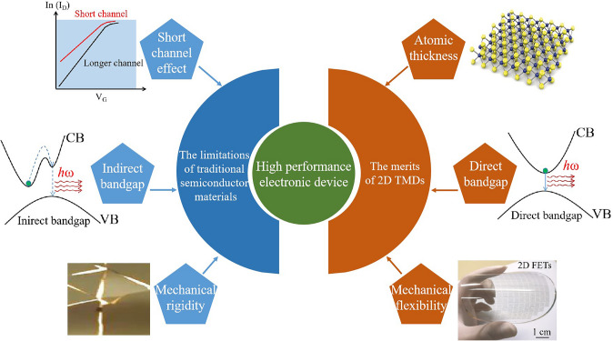
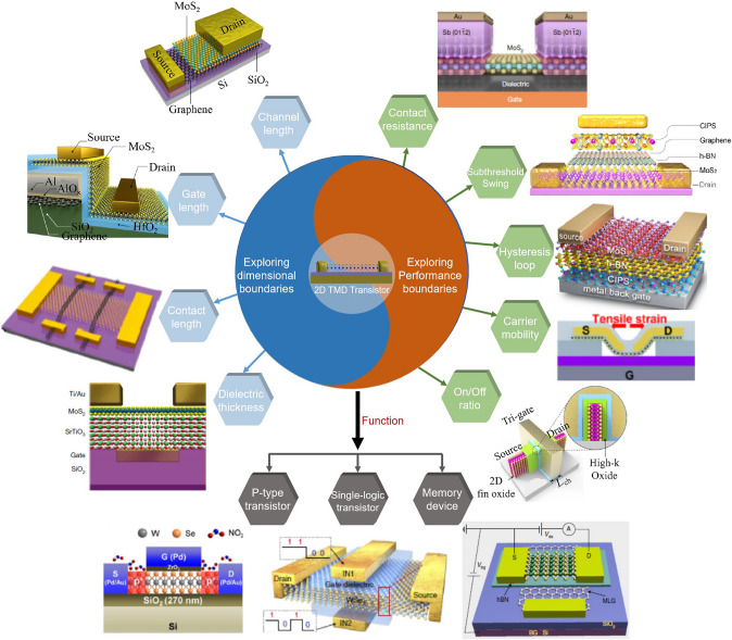
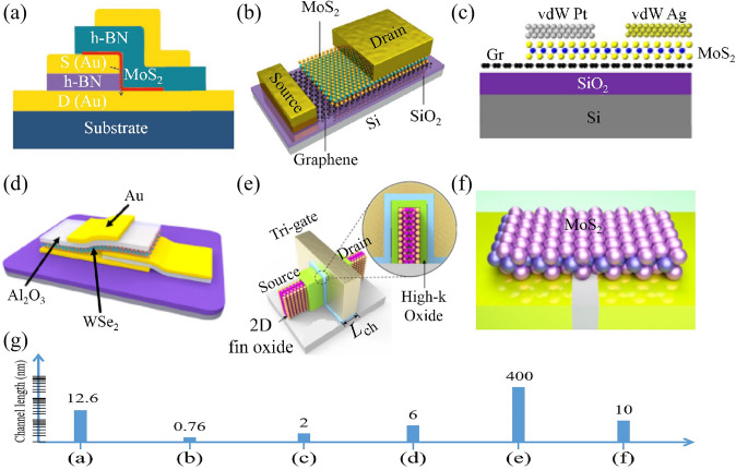
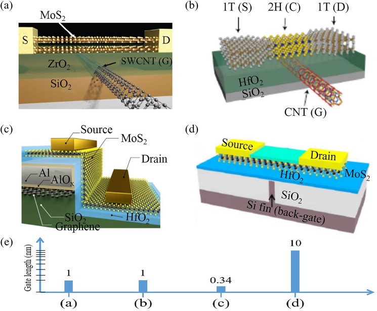
Two-dimensional (2D) transition metal dichalcogenides (TMDs) allow for atomic-scale manipulation, challenging the conventional limitations of semiconductor materials. This capability may overcome the short-channel effect, sparking significant advancements in electronic devices that utilize 2D TMDs. Exploring the dimension and performance limits of transistors based on 2D TMDs has gained substantial importance. This review provides a comprehensive investigation into these limits of the single 2D-TMD transistor. It delves into the impacts of miniaturization, including the reduction of channel length, gate length, source/drain contact length, and dielectric thickness on transistor operation and performance. In addition, this review provides a detailed analysis of performance parameters such as source/drain contact resistance, subthreshold swing, hysteresis loop, carrier mobility, on/off ratio, and the development of p-type and single logic transistors. This review details the two logical expressions of the single 2D-TMD logic transistor, including current and voltage. It also emphasizes the role of 2D TMD-based transistors as memory devices, focusing on enhancing memory operation speed, endurance, data retention, and extinction ratio, as well as reducing energy consumption in memory devices functioning as artificial synapses. This review demonstrates the two calculating methods for dynamic energy consumption of 2D synaptic devices. This review not only summarizes the current state of the art in this field but also highlights potential future research directions and applications. It underscores the anticipated challenges, opportunities, and potential solutions in navigating the dimension and performance boundaries of 2D transistors.

Keywords: Artificial synapses; Dimension limits; Memory devices; Performance limits; Two-dimensional transistors.


Conflict of interest statement

The authors declare no interest conflict. They have no known competing financial interests or personal relationships that could have appeared to influence the work reported in this paper.

Figures

Fig. 1
Fig. 1
The limitations of traditional semiconductor materials and the merits of 2D TMDs for high performance electronic device. The diagram of flexible 2D FETs. Reproduced with permission. Reference [10] Copyright 2022, Springer Nature
Fig. 2
Fig. 2
Demonstration of dimension and performance limits in 2D TMD transistors. Channel length diagram. Reproduced with permission. Reference [27] Copyright 2021, Springer Nature. Gate length diagram. Reproduced with permission. Reference [28] Copyright 2022, Springer Nature. Contact length diagram. Reproduced with permission. Reference [29] Copyright 2023, Springer Nature. Dielectric thickness diagram. Reproduced with permission. Reference [30] Copyright 2022, Springer Nature. Contact resistance diagram. Reproduced with permission. Reference [31] Copyright 2023, Springer Nature. Subthreshold swing diagram. Reproduced with permission. Reference [32] Copyright 2021, Springer Nature. Hysteresis loop diagram. Reproduced with permission. Reference [33] Copyright 2023, American Chemical Society. Carrier mobility diagram. Reproduced with permission. Reference [34] Copyright 2023, American Chemical Society. On/Off ratio diagram. Reproduced with permission. Reference [35] Copyright 2023, Springer Nature. P-type transistor diagram. Reproduced with permission. Reference [36] Copyright 2022, Wiley–VCH Verlag. Single-logic transistor diagram. Reproduced with permission. Reference [37] Copyright 2021, Springer Nature. Memory device diagram. Reproduced with permission. Reference [38] Copyright 2021, Springer Nature
Fig. 3
Fig. 3
Comparison of conventional bulk material and 2D TMD material. a Bulk material. Reproduced with permission. Reference [1] Copyright 2022, Elsevier. b 2D TMD material. Reproduced with permission. Reference [39] Copyright 2011, Springer Nature
Fig. 4
Fig. 4
Fabrication methods of monolayer TMDs. a Micromechanical exfoliation method. Reproduced with permission. Reference [51] Copyright 2022, Royal Society of Chemistry. b Chemical vapor deposition method. Reproduced with permission. Reference [47] Copyright 2022, Wiley
Fig. 5
Fig. 5
Demonstration of the dimensions of 2D transistors, such as dielectric thickness, channel length, gate length, and contact length. a Top-gate transistor. b Back-gate transistor
Fig. 6
Fig. 6
Scaling down the channel length of transistors. a 2D vertical-channel transistors. Reproduced with permission. Reference [65] Copyright 2020, Wiley. b Vertical transistor with a sub-1-nm channel. Reproduced with permission. Reference [27] Copyright 2021, Springer Nature. c Sub-2 nm vertical-channel transistors. Reproduced with permission. Reference [66] Copyright 2023, American Chemical Society. d Monolayer WSe2 sloping-channel transistors. Reproduced with permission. Reference [67] Copyright 2023, American Chemical Society. e 2D fin field-effect transistors. Reproduced with permission. Reference [35] Copyright 2023, Springer Nature. f 2D devices with ultraflat sub-10 nm gap electrodes. Reproduced with permission. Reference [68] Copyright 2021, American Chemical Society. g Channel lengths of above 2D transistors
Fig. 7
Fig. 7
Scaling down the gate length of transistors. a MoS2 transistors with 1-nm gate lengths. Reproduced with permission. Reference [92] Copyright 2016, American Association for the Advancement of Science. b 1 T′/2H MoTe2 FET with a CNT gate. Reproduced with permission. Reference [93] Copyright 2019, Springer Nature. c Vertical MoS2 transistors with 0.34 nm monolayer graphene edge gate. Reproduced with permission. Reference [28] Copyright 2022, Springer Nature. d MoS2 Transistor with 10-nm Si fin gate length. Reproduced with permission. Reference [96] Copyright 2019, Institute of Electrical and Electronics Engineers Inc. e Gate lengths of above 2D transistors
Fig. 8
Fig. 8
Scaling down the contact length of transistors. a Ultrascaled contacts for monolayer MoS2 FET. Reproduced with permission. Reference [109] Copyright 2023, American Chemical Society. b PtSe2 FET with PtTe2 edge contacts. Reproduced with permission. Reference [111] Copyright 2022, Elsevier. c MoS2 transistors using in situ edge contacts. Reproduced with permission. Reference [112] Copyright 2019, American Chemical Society. d MoS2 FET with single-walled-carbon-nanotube contacts. Reproduced with permission. Reference [29] Copyright 2023, Springer Nature. e MoS2 FET with one-dimensional edge contacts. Reproduced with permission. Reference [113] Copyright 2019, American Chemical Society. f MoTe2 FET with phase-transition contacts. Reproduced with permission. Reference [116] Copyright 2020, Wiley–VCH Verlag. g Contact lengths of above 2D transistors
Fig. 9
Fig. 9
Scaling down the dielectric thickness of transistors. a Laser-writable high-k dielectric for van der Waals nanoelectronics. Reproduced with permission. Reference [129] Copyright 2019, American Association for the Advancement of Science. b The hybrid HfO2/Sb2O3 dielectrics integrated on 2D MoS2. Reproduced with permission. Reference [130] Copyright 2023, Springer Nature. c Bi2O2Se transistor with Bi2SeO5 dielectric nanosheets. Reproduced with permission. Reference [131] Copyright 2023, Springer Nature. d Back-gate MoS2 four-probe FETs device. Reproduced with permission. Reference [132] Copyright 2023, Springer Nature. e MoS2 back-gated FET with SrTiO3 dielectric material. Reproduced with permission. Reference [30] Copyright 2022, Springer Nature. f MoS2 FET with hybrid PTCDA/HfO2 gate stack. Reproduced with permission. Reference [133] Copyright 2019, Springer Nature. g Bi2O2Se transistor with Bi2SeO5 dielectric nanosheets. Reproduced with permission. Reference [134] Copyright 2022, Springer Nature. h WSe2 FET using 2D-BN dielectric interface. Reproduced with permission. Reference [150] Copyright 2019, Springer Nature. i Dielectric thickness of above 2D transistors. j Dielectric constants of above 2D transistors
Fig. 10
Fig. 10
Contact resistance reduction of 2D transistors involves four strategies such as novel contact materials, doping engineering, interface engineering, and phase-change engineering. a The quantum limit in MoS2 FET. Reproduced with permission. Reference [31] Copyright 2023, Springer Nature. b MoS2 FET with semimetal (Bi) contacts. Reproduced with permission. Reference [156] Copyright 2021, Springer Nature. c Double-gate InSe FET. Reproduced with permission. Reference [171] Copyright 2023, Springer Nature. d WSe2 FET with degenerately p-doped WSe2 (Nb0.005W0.995Se2) contacts. Reproduced with permission. Reference [172] Copyright 2016, American Chemical Society. e ZrTe2-contacted MoS2 transistor. Reproduced with permission. Reference [160] Copyright 2023, American Chemical Society. f Ideal spacer doping layer for 2D devices. Reproduced with permission. Reference [164] Copyright 2023, American Chemical Society. g MoTe2 device with a 1 T'/2H phase homojunction. Reproduced with permission. Reference [173] Copyright 2015, American Association for the Advancement of Science. h 2D MoGe2N4 FET with Mxene contacts. Reproduced with permission. Reference [174] Copyright 2023, Royal Society of Chemistry. i WSe2 FET with VSe2 contact. Reproduced with permission. Reference [152] Copyright 2023, Springer Nature. j Contact resistance of above 2D transistors
Fig. 11
Fig. 11
Subthreshold swing reduction of 2D transistors involves negative capacitance effect, resistive gate effect, tunnel effect, Dirac-source effect, and impact ionization effect. a MoS2 NC-FET. Reproduced with permission. Reference [211] Copyright 2020, Wiley-Blackwell. b CIPS/MoS2 vdW NC-FET. Reproduced with permission. Reference [212] Copyright 2019, Springer Nature. c MoS2 NC-FET. Reproduced with permission. Reference [213] Copyright 2018, Springer Nature. d MoS2/h-BN/graphene/CIPS vdW FeFET. Reproduced with permission. Reference [32] Copyright 2021, Springer Nature. e Atomic threshold switching MoS2 FET. Reproduced with permission. Reference [214] Copyright 2021, Wiley–VCH Verlag. f MoS2 TFET. Reproduced with permission. Reference [215] Copyright 2015, Springer Nature. g MoS2/Graphene Dirac-source FET. Reproduced with permission. Reference [209] Copyright 2021, American Chemical Society. h Nanoscale vertical impact-ionization transistor. Reproduced with permission. Reference [207] Copyright 2020, American Chemical Society. i Subthreshold swings of above 2D transistors
Fig. 12
Fig. 12
Hysteresis reduction of 2D transistors includes four strategies such as surface passivation, dielectric engineering, encapsulation, and post-fabrication treatments. a MoS2 FET with hBN passivation layer. Reproduced with permission. Reference [238] Copyright 2015, Springer Nature. b MoS2 FET with HfOx dielectric. Reproduced with permission. Reference [239] Copyright 2022, Springer Nature. c MoS2 negative-capacitance FET with h-BN/CuInP2S6 dielectric. Reproduced with permission. Reference [33] Copyright 2023, American Chemical Society. d Single-layer MoS2 FET with post-fabrication treatment. Reproduced with permission. Reference [39] Copyright 2011, Springer Nature. e Hysteresis of above 2D transistors
Fig. 13
Fig. 13
Carrier mobility enhancement in 2D transistors involves material quality improvement, surface functionalization, dielectric engineering, strain engineering, and device architecture optimization. a Rhombohedral-stacked bilayer WS2 FET. Reproduced with permission. Reference [255] Copyright 2023, American Association for the Advancement of Science. b MoS2 FET coupled with 2D organic frameworks. Reproduced with permission. Reference [256] Copyright 2023, Wiley-Blackwell. c CsPbBr3 precipitation on a MoS2 FET. Reproduced with permission. Reference [249] Copyright 2023, American Chemical Society. d MoS2 FET with high dielectric constant of Bi2SeO2. Reproduced with permission. Reference [131] Copyright 2023, Springer Nature. e Dual-gate MoS2 FeFET. Reproduced with permission. Reference [257] Copyright 2020, Wiley-Blackwell. f WSe2 FET using conformal BN dielectric interface. Reproduced with permission. Reference [150] Copyright 2019, Springer Nature. g Crested two-dimensional transistors. Reproduced with permission. Reference [258] Copyright 2019, Springer Nature. h Strained MoS2 transistor. Reproduced with permission. Reference [34] Copyright 2023, American Chemical Society. i MoS2 transistor with air-gap structure. Reproduced with permission. Reference [151] Copyright 2023, Springer Nature. j Carrier mobilities of above 2D transistors
Fig. 14
Fig. 14
Strategies to enhance the on/off ratio of 2D transistors involve gate engineering, contact optimization, defect control, device architecture optimization. a High-κ perovskite membranes as insulators for two-dimensional transistors. Reproduced with permission. Reference [30] Copyright 2022, Springer Nature. b Bi-contacted MoS2 field effect transistors. Reproduced with permission. Reference [273] Copyright 2024, Science China Press. c High performance MoS2 transistor fabricated via residue-free transfer. Reproduced with permission. Reference [191] Copyright 2023, Springer Nature. d Defect control for 2D transistors. Reproduced with permission. Reference [23] Copyright 2021, Springer Nature. e High performance MoS2 transistor fabricated via modified chemical vapor deposition. Reproduced with permission. Reference [274] Copyright 2020, Springer Nature. f 2D fin field-effect transistors. Reproduced with permission. Reference [35] Copyright 2023, Springer Nature. g The on/off ratios of above 2D transistors
Fig. 15
Fig. 15
P-type transistors. a NO2 molecules for p-type dopants of WSe2. Reproduced with permission. Reference [36] Copyright 2022, Wiley–VCH Verlag. b V-doped WSe2 by mixing W with V precursors. Reproduced with permission. Reference [290] Copyright 2020, Wiley–VCH Verlag. c Ultrascaled p-type FET based on WSe2/WOxSey heterostructure. Reproduced with permission. Reference [291] Copyright 2023, American Chemical Society. d The p-type MoTe2-based transistor fabrication. Reproduced with permission. Reference [176] Copyright 2023, Springer Nature. e The MoS2/CNT heterojunction transistor. Reproduced with permission. Reference [292] Copyright 2023, Springer Nature. f WSe2 FET after laser scanning. Reproduced with permission. Reference [285] Copyright 2019, American Chemical Society. g Atomic resolution images of Pt on multilayer WSe2. Reproduced with permission. Reference [159] Copyright 2022, Springer Nature
Fig. 16
Fig. 16
Single logic transistor. a Dual-gate MoS2 transistor. Reproduced with permission. Reference [126] Copyright 2019, Springer Nature. b Dual-gate WSe2 transistor. Reproduced with permission. Reference [297] Copyright 2022, Springer Nature. c Dual-gate WSe2 transistor. Reproduced with permission. Reference [37] Copyright 2021, Springer Nature. d WSe2 floating gate transistor. Reproduced with permission. Reference [298] Copyright 2023, American Chemical Society. e MoS2 floating gate transistor. Reproduced with permission. Reference [299] Copyright 2020, Springer Nature. f Reconfigurable van der Waals ferroelectric transistor. Reproduced with permission. Reference [281] Copyright 2023, American Chemical Society
Fig. 17
Fig. 17
Ultrafast memory devices. a The floating-gate memory device with atomically sharp interface. Reproduced with permission. Reference [308] Copyright 2021, Springer Nature. b Ultrafast semi-floating gate homojunctions. Reproduced with permission. Reference [314] Copyright 2023, Wiley-Blackwell. c Ultrafast flash memory based on van der Waals heterostructures. Reproduced with permission. Reference 38] Copyright 2021, Springer Nature. d Ultrafast MoS2 floating memory. Reproduced with permission. Reference [315] Copyright 2022. e Ultrafast WSe2 bipolar flash memory. Reproduced with permission. Reference [316] Copyright 2023, Springer Nature. f Ultrafast flash memory based on phase-engineered edge contacts. Reproduced with permission. Reference [82] Copyright 2015, Springer Nature. g Ultrafast van der Waals memory with PbI2 as the charge trap layer. Reproduced with permission. Reference [313] Copyright 2023, Wiley-Blackwell. h Polarized Tunneling Transistor for Ultrafast Memory. Reproduced with permission. Reference [309] Copyright 2023, American Chemical Society. i Ultrafast flash memory based on a duplex two-dimensional material structure. Reproduced with permission. Reference [317] Copyright 2023, Springer Nature. j PZT-enabled MoS2 floating gate transistor for ultrafast flash memory. Reproduced with permission. Reference [310] Copyright 2023, American Chemical Society

References

    1. T. Wei, Z. Han, X. Zhong, Q. Xiao, T. Liu et al., Two dimensional semiconducting materials for ultimately scaled transistors. iScience 25, 105160 (2022). 10.1016/j.isci.2022.105160 - PMC - PubMed
    1. C. Liu, H. Chen, S. Wang, Q. Liu, Y.-G. Jiang et al., Two-dimensional materials for next-generation computing technologies. Nat. Nanotechnol. 15, 545–557 (2020). 10.1038/s41565-020-0724-3 - PubMed
    1. K.P. O’Brien, C.H. Naylor, C. Dorow, K. Maxey, A.V. Penumatcha et al., Process integration and future outlook of 2D transistors. Nat. Commun. 14, 6400 (2023). 10.1038/s41467-023-41779-5 - PMC - PubMed
    1. W. Li, H. Shen, H. Qiu, Y. Shi, X. Wang, Two-dimensional semiconductor transistors and integrated circuits for advanced technology nodes. Natl. Sci. Rev. 11, nwae001 (2024). 10.1093/nsr/nwae001 - PMC - PubMed
    1. L. Yin, R. Cheng, J. Ding, J. Jiang, Y. Hou et al., Two-dimensional semiconductors and transistors for future integrated circuits. ACS Nano 18, 7739–7768 (2024). 10.1021/acsnano.3c10900 - PubMed

LinkOut - more resources