

Visual and Quantitative Analysis of the Trapping Volume in Dielectrophoresis of Nanoparticles
- PMID: 39133749
- PMCID: PMC11342383
- DOI: 10.1021/acs.nanolett.4c02903
Visual and Quantitative Analysis of the Trapping Volume in Dielectrophoresis of Nanoparticles
Abstract
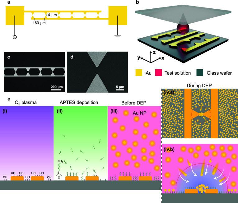
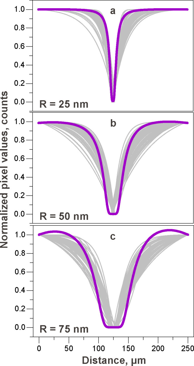
Nanoparticle manipulation requires careful analysis of the forces at play. Unfortunately, traditional force measurement techniques based on the particle velocity do not provide sufficient resolution, while balancing approaches involving counteracting forces are often cumbersome. Here, we demonstrate that a nanoparticle dielectrophoretic response can be quantitatively studied by a straightforward visual delineation of the dielectrophoretic trapping volume. We reveal this volume by detecting the width of the region depleted of gold nanoparticles by the dielectrophoretic force. Comparison of the measured widths for various nanoparticle sizes with numerical simulations obtained by solving the particle-conservation equation shows excellent agreement, thus providing access to the particle physical properties, such as polarizability and size. These findings can be further extended to investigate various types of nano-objects, including bio- and molecular aggregates, and offer a robust characterization tool that can enhance the control of matter at the nanoscale.
Keywords: dielectrophoresis; electrokinetic effects; force; nanoparticles; polarizability; trapping volume.
Conflict of interest statement
The authors declare no competing financial interest.
Figures


 .
.
Similar articles
-
Selective Manipulation of Biomolecules with Insulator-Based Dielectrophoretic Tweezers.ACS Appl Nano Mater. 2020 Jan 24;3(1):797-805. doi: 10.1021/acsanm.9b02302. Epub 2020 Jan 3. ACS Appl Nano Mater. 2020. PMID: 32587952 Free PMC article.
-
Parameter optimization for positive dielectrophoretic trapping force on ZnO nanoparticles through simulation.J Nanosci Nanotechnol. 2012 Feb;12(2):1152-6. doi: 10.1166/jnn.2012.4706. J Nanosci Nanotechnol. 2012. PMID: 22629911
-
Experimental and theoretical study of dielectrophoretic particle trapping in arrays of insulating structures: Effect of particle size and shape.Electrophoresis. 2015 May;36(9-10):1086-97. doi: 10.1002/elps.201400408. Epub 2015 Mar 16. Electrophoresis. 2015. PMID: 25487065
-
Electric field-induced effects on neuronal cell biology accompanying dielectrophoretic trapping.Adv Anat Embryol Cell Biol. 2003;173:III-IX, 1-77. doi: 10.1007/978-3-642-55469-8. Adv Anat Embryol Cell Biol. 2003. PMID: 12901336 Review.
-
Dielectrophoresis for manipulation of micro/nano particles in microfluidic systems.Anal Bioanal Chem. 2010 Jan;396(1):401-20. doi: 10.1007/s00216-009-2922-6. Epub 2009 Jul 4. Anal Bioanal Chem. 2010. PMID: 19578834 Review.
Cited by
-
Insulator-Based Dielectrophoresis for Purifying Semiconductor Industry-Compatible Chemicals with Trace Nanoparticles.JACS Au. 2025 May 15;5(5):2342-2349. doi: 10.1021/jacsau.5c00307. eCollection 2025 May 26. JACS Au. 2025. PMID: 40443887 Free PMC article.
-
The Dielectrophoretic Interactions of Curved Particles in a DC Electric Field.Micromachines (Basel). 2025 May 20;16(5):596. doi: 10.3390/mi16050596. Micromachines (Basel). 2025. PMID: 40428722 Free PMC article.
References
-
- Ramos A.; Morgan H.; Green N. G.; Castellanos A. Ac Electrokinetics: A Review of Forces in Microelectrode Structures. J. Phys. D: Appl. Phys. 1998, 31 (18), 2338–2353. 10.1088/0022-3727/31/18/021. - DOI
-
- Schoch R. B.; Han J.; Renaud P. Transport Phenomena in Nanofluidics. Rev. Mod. Phys. 2008, 80 (3), 839–883. 10.1103/RevModPhys.80.839. - DOI
-
- Squires T. M.; Quake S. R. Microfluidics: Fluid Physics at the Nanoliter Scale. Rev. Mod. Phys. 2005, 77 (3), 977–1026. 10.1103/RevModPhys.77.977. - DOI
LinkOut - more resources
Full Text Sources
