

Determination of the significance of atomic concentration on surface properties of Ba x Mg1- x F2 alloy coatings via microscopic and spectroscopic techniques
- PMID: 39161445
- PMCID: PMC11331579
- DOI: 10.1039/d4ra05211k
Determination of the significance of atomic concentration on surface properties of Ba x Mg1- x F2 alloy coatings via microscopic and spectroscopic techniques
Abstract
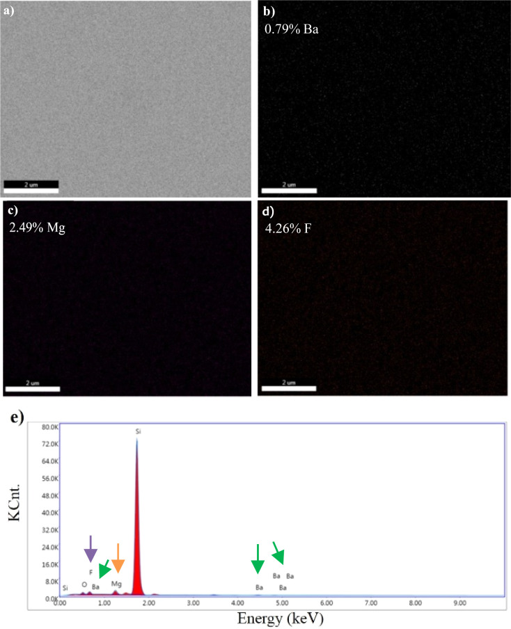
Both BaF2 and MgF2 compounds and Ba x Mg1-x F2 alloy thin films were deposited on glass and silicon (Si) substrates in nanometric sizes (100 ± 10 nm) in a high vacuum environment by radio frequency (rf) magnetron sputtering. Using BaF2 (99% purity) and MgF2 (99% purity) target materials and adjusting the power levels applied to these targets, Ba x Mg1-x F2 alloy coatings at different atomic concentrations were formed under the same vacuum conditions. The microstructure and surface characteristics of the samples were analysed with the help of spectroscopic and microscopic methods. For the surface characterization, with scanning acoustic microscopy (SAM), 2-dimensional surface acoustic images of the samples were mapped, the surface acoustic impedance values were determined, and information about the micro hardness of the materials was obtained. Surface roughness values and grain sizes were obtained by taking 3-dimensional surface images of investigated materials using atomic force microscopy (AFM). Average nanometric particle sizes were determined for each sample with scanning electron microscopy (SEM), therefore, information about surface homogeneity was obtained. For the microstructural characterization, quantitative elemental analysis was performed using scanning electron microscopy/energy dispersive X-ray spectroscopy (SEM-EDS), and stoichiometric ratios of atomic compositions were identified. By evaluating the data obtained from the microscopic and spectroscopic measurements, the effect of the atomic concentration parameter on the morphological properties of the material was determined. The usability of the produced binary fluoride alloy thin film coatings is promising for emerging optoelectronic, ceramic industry, biomedical and surface acoustic wave applications.
This journal is © The Royal Society of Chemistry.
Conflict of interest statement
There are no conflicts to declare.
Figures


References
-
- Ebralidze I. I., Laschuk N. O., Poisson J. and Zenkina O. V., Colorimetric Sensors and Sensor Arrays, Springer, Amsterdam, The Netherlands, 1st edn, 2019
-
- Palla-Papavlu A. Voicu S. I. Dinescu M. Chemosensors. 2021;9:105.
-
- Liu R. Li X. Hu X. Dong H. Surf. Coat. Technol. 2013;232:906–911.
-
- Wang Q. Zhou F. Wang C. Yuen M. F. Wang M. Qian T. Matsumoto M. Yan J. Mater. Chem. Phys. 2015;158:74–81.
LinkOut - more resources
Full Text Sources
Miscellaneous