

Polarized Raman mapping and phase-transition by CW excitation for fast purely optical characterization of VO2 thin films
- PMID: 39164376
- PMCID: PMC11336108
- DOI: 10.1038/s41598-024-70301-0
Polarized Raman mapping and phase-transition by CW excitation for fast purely optical characterization of VO2 thin films
Abstract
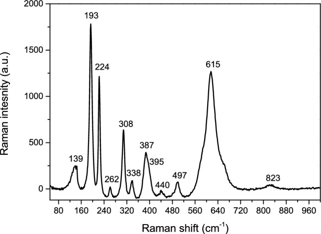
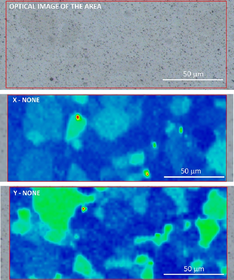
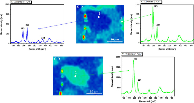
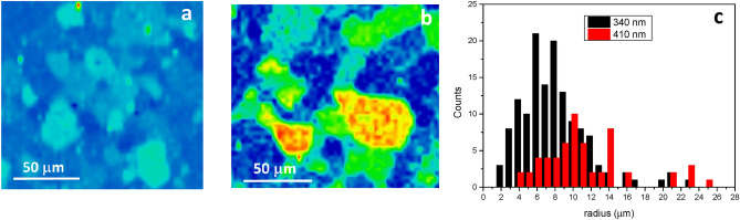
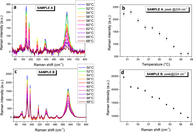
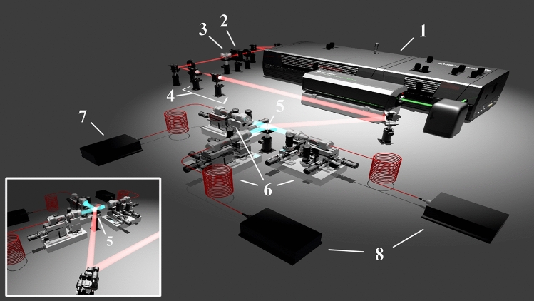
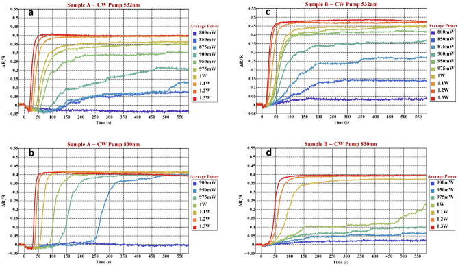
Vanadium dioxide has attracted much interest due to the drastic change of the electrical and optical properties it exhibits during the transition from the semiconductor state to the metallic state, which takes place at a critical temperature of about 68 °C. Much study has been especially devoted to developing advanced fabrication methodologies to improve the performance of VO2 thin films for phase-change applications in optical devices. Films structural and morphological characterisation is normally performed with expensive and time consuming equipment, as x-ray diffractometers, electron microscopes and atomic force microscopes. Here we propose a purely optical approach which combines Polarized Raman Mapping and Phase-Transition by Continuous Wave Optical Excitation (PTCWE) to acquire through two simple measurements structural, morphological and thermal behaviour information on polycrystalline VO2 thin films. The combination of the two techniques allows to reconstruct a complete picture of the properties of the films in a fast and effective manner, and also to unveil an interesting stepped appearance of the hysteresis cycles probably induced by the progressive stabilization of rutile metallic domains embedded in the semiconducting monoclinic matrix.
Keywords: Continuous wave excitation; Phase transition; Polarized Raman; VO2 thin films.
© 2024. The Author(s).
Conflict of interest statement
The authors declare no competing interests.
Figures
References
-
- Morin, F. J. Oxides Which Show a Metal-to-Insulator Transition at the Neel Temperature. Phys. Rev. Lett.3, 34–36 (1959).10.1103/PhysRevLett.3.34 - DOI
-
- Kucharcsyyk, D. & Niklewski, T. J. Accurate X-ray determination of the lattice parameters and the thermal expansion Coefficients of VO2 near the transition temperature. Appl Cristallogr.12(370), 373 (1979).
-
- Goodenough, J. B. The two components of the crystallographic transition in VO2. J. Solid Chem.3, 490–500 (1971).10.1016/0022-4596(71)90091-0 - DOI
-
- Shao, Z., Cao, X., Luo, H. & Jin, P. Recent progress in the phase-transition mechanism and modulation of vanadium dioxide materials. NPG Asia Mater.10, 581–605 (2018).10.1038/s41427-018-0061-2 - DOI
-
- Shvets, P., Shabanov, A., Maksimova, K. & Goikhman, A. Micro-Raman mapping of VO2 (T) microcrystals orientation. Vibrat. Spectrosc.118, 103328–103336 (2022).10.1016/j.vibspec.2021.103328 - DOI
LinkOut - more resources
Full Text Sources
