Review
. 2024 Aug 13;17(16):4029.
doi: 10.3390/ma17164029.

Perovskite versus Standard Photodetectors

Affiliations
Review

Perovskite versus Standard Photodetectors

Antoni Rogalski et al. Materials (Basel). .

Abstract

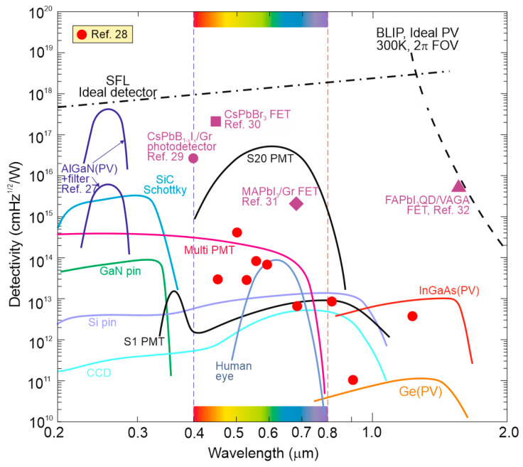
Perovskites have been largely implemented into optoelectronics as they provide several advantages such as long carrier diffusion length, high absorption coefficient, high carrier mobility, shallow defect levels and finally, high crystal quality. The brisk technological development of perovskite devices is connected to their relative simplicity, high-efficiency processing and low production cost. Significant improvement has been made in the detection performance and the photodetectors' design, especially operating in the visible (VIS) and near-infrared (NIR) regions. This paper attempts to determine the importance of those devices in the broad group of standard VIS and NIR detectors. The paper evaluates the most important parameters of perovskite detectors, including current responsivity (R), detectivity (D*) and response time (τ), compared to the standard photodiodes (PDs) available on the commercial market. The conclusions presented in this work are based on an analysis of the reported data in the vast pieces of literature. A large discrepancy is observed in the demonstrated R and D*, which may be due to two reasons: immature device technology and erroneous D* estimates. The published performance at room temperature is even higher than that reported for typical detectors. The utmost D* for perovskite detectors is three to four orders of magnitude higher than commercially available VIS PDs. Some papers report a D* close to the physical limit defined by signal fluctuations and background radiation. However, it is likely that this performance is overestimated. Finally, the paper concludes with an attempt to determine the progress of perovskite optoelectronic devices in the future.

Keywords: HOT devices; colloidal quantum dot (CQD) detectors; fundamental limits of photodetector performance (SFL and BLIP); perovskite photodetectors; photogating effect.


Conflict of interest statement

The authors declare no conflicts of interest.

Figures

Figure 2
Figure 2
Properties of perovskite materials: (a) APbI3 tolerance factor for selected cations in the A-site [6]; (b) photoluminescence energy for doped CsPb1−xMxBr3 nanocrystals versus the lattice vector for M = Sn2+, Zn2+, Cd2+ [8]; (c) the band structure of typical defect-intolerant semiconductors (e.g., GaAs, CdSe, InP) (left) and defect-tolerant halide perovskite (e.g., APbX3) (right) [9]; (d) the T50 lifetimes versus initial radiance. The solid dots are based on the T50 measurements, while the open circles depict the extrapolated T50 lifetimes for the ongoing measurements at medium and low current densities [10].
Figure 4
Figure 4
Comparison of room temperature D* for perovskite photodetectors [28,29,30,31,32] with standard market detectors (AlGaN, Si, Ge, InGaAs PDs and PMTs) in the wavelength range 0.2–2 μm. The ultimate SFL and BLIP are also shown. PV—photovoltaic detector, PMT—photomultiplier tube, FET—field effect transistor. The perovskite photodetectors’ D* marked in magenta is probably overestimated.
Figure 1
Figure 1
Perovskite structures: (a) the 3D ABX3, where A corresponds to the FA, MA, Cs+ cations, B denotes Sn2+ and Pb2+ metal cations and X stands for Br, Cl, I halogen anions (after Ref. [4]); (b) 2D (RNH3)2[ABX3]nBX4 (n = 0, 1, 2) and 3D ABX3 (n = ∞) perovskite structures, where A′ represents the RNH3+ cations (after Ref. [4]); (c) molecular structures of different organic amine cations.
Figure 3
Figure 3
Optoelectronic material properties for the thin−film perovskite technologies: (a) absorption coefficient; (b) open−circuit voltage for the market technologies; and (c) binding energy and diffusion length for selected PV materials (after Ref. [15]).
Figure 5
Figure 5
Timeline of perovskite UV–VIS–NIR photodetector development (adapted with Ref. [37] with the additions of VIS–NIR PD array and flexible VIS-blind UV PD).
Figure 6
Figure 6
Perovskite PV detectors: (a) band diagram and principle operation (favourable energy band alignment affects the carriers’ transport to the device’s contacts); and (b) bandgap for perovskite materials.
Figure 7
Figure 7
MOSFET operation: (a) output source-drain current curves for selected gate biases; (bd) variation of the conduction channel versus VDS; (b) at linear; (c) at pinch-off; (d) in the saturation regimes.
Figure 8
Figure 8
Photogating effect: (a) energy band structure under light condition (holes are trapped at the band edge acting as a local gate, while the field-effect drives more electrons in the channel, generating a photocurrent; if the electron lifetime exceeds the time it takes for the electron to transit device, then the trapped holes time allows the electrons to circulate resulting in high gain, (bd) photogating effect in LDS based photodetectors; (b) the hybrid PT operation, (c) closed channel under light conditions, and (d) photoconductive gain.
Figure 9
Figure 9
Pros and cons of the perovskite based photodetectors: PV, PC and PT.
Figure 10
Figure 10
The mixed single crystal MAPbBr3−xClx and MAPbI3−xBrx narrowband perovskite detectors (a) device design, (b) normalized EQE versus selected halide compositions [measured for −1 V (after Ref. [49])].
Figure 11
Figure 11
Typical perovskite PD: (a) heterojunction device design—structure incorporates ITO transparent conductive (ohmic) electrode, HTL (PEDOT:PSS), absorber (MAPbI3 − xClx), ETL (PCBM), and Al ohmic contact, (b) dark J-V and under illumination, (c) EQE and spectral detectivity with Si PD for comparison (after Ref. [51]).
Figure 12
Figure 12
The 34 × 38 mm2 MAPbBr3 SCR based 27 × 27 array: (a) sensors’ picture, (b) PC’s EQE and D* versus wavelength for 4 V (after Ref. [52]).
Figure 13
Figure 13
Perovskite PTs: (a) hybrid design based on graphene-CsPbBr3 − xIx NCs and (b) R and D* for selected light powers for 405 nm and VDS = 1 V and VGS = −60 V (after Ref. [29]); (c) FET NIR photodetector (λ = 1550 nm) based on FAPbI3 QD/VAGA and (d) power density-dependent R and D* (after Ref. [32]); (e) the PT design with a CNT/CsPbBr3-QD channel and (f) array with wire bonding on a printed circuit board (5 mm scale bar) (after Ref. [43]); (g) PT based on Sr2Nb3O10 (SNO) NSs and (h) the R for selected thicknesses for 1 V (after Ref. [54]).
Figure 14
Figure 14
The flexible/self-powered perovskite based detector: (a) design, (b) device on the rounded surface (after Ref. [56]).
Figure 15
Figure 15
Detectivity (a) and current responsivity (b) versus voltage for device’ designs based on the perovskite materials published up to 2017. “w.Graphene” and similar (w.CNT, w.PbS, etc.) denote hybrid photodetectors with other materials. PD—photodiode; PC—photoconductor; PT—phototransistor; PF—polycrystalline film; BC—bulk crystal; NS—nanosheet; NW—nanowire; NC—nanocrystal (after Ref. [28]).
Figure 16
Figure 16
Comparison of R and D* for hybrid perovskite based photodetectors at 300 K. For comparison purposes, the typical VIS PDs performance is also marked [29,30,31,32,43,44,45,46,60,61,62,63,64,65,66,67,68].
Figure 17
Figure 17
Detectivity dependence on gain for selected perovskite based detectors at 300 K. The are is collected after the following Refs. [29,30,32,39,40,41,43,44,45,46,52,54,69,70,71,72,73,74,75,76]. Theoretical predictions for SFL for 400‒800 nm wavelength range are also marked. PC—photoconductor, PD—photodiode, FET—field effect transistor, MSM—metal–semiconductor–metal.
Figure 18
Figure 18
The room temperature current responsivity dependence on the response time for the perovskite-based hybrid photodetectors. The measured data were extracted from selected papers.

References

    1. Miyasaka T. Perovskite Photovoltaics and Optoelectronics. From Fundamentals to Advanced Applications. Wiley-VCH GmbH; Weinheim, Germany: 2022.
    1. Ding L. Perovskite Materials and Devices. Wiley-VCH GmbH; Weinheim, Germany: 2022.
    1. Sutherland B.R., Sargen E.H. Perovskite photonic sources. Nat. Photonics. 2016;10:295–302. doi: 10.1038/nphoton.2016.62. - DOI
    1. Jagielski J., Kumar S., Yu W.-Y., Shih C.-J. Layer-controlled two-dimensional perovskites: Synthesis and optoelectronics. J. Mater. Chem. C. 2017;5:5610–5627. doi: 10.1039/C7TC00538E. - DOI
    1. Goldschmidt V.M. Die Gesetze der Krystallochemie. Die Naturwissenschaften. 1926;14:477–485. doi: 10.1007/BF01507527. - DOI

LinkOut - more resources