. 2024 Aug 14;17(16):4048.
doi: 10.3390/ma17164048.

Real-Time Spectroscopic Ellipsometry for Flux Calibrations in Multi-Source Co-Evaporation of Thin Films: Application to Rate Variations in CuInSe2 Deposition

Affiliations

Real-Time Spectroscopic Ellipsometry for Flux Calibrations in Multi-Source Co-Evaporation of Thin Films: Application to Rate Variations in CuInSe2 Deposition

Dhurba R Sapkota et al. Materials (Basel). .

Abstract

Flux calibrations in multi-source thermal co-evaporation of thin films have been developed based on real-time spectroscopic ellipsometry (RTSE) measurements. This methodology has been applied to fabricate CuInSe2 (CIS) thin film photovoltaic (PV) absorbers, as an illustrative example, and their properties as functions of deposition rate have been studied. In this example, multiple Cu layers are deposited step-wise onto the same Si wafer substrate at different Cu evaporation source temperatures (TCu). Multiple In2Se3 layers are deposited similarly at different In source temperatures (TIn). Using RTSE, the Cu and In2Se3 deposition rates are determined as functions of TCu and TIn. These rates, denoted Reff, are measured in terms of effective thickness which is the volume per planar substrate area and accounts for surface roughness variations with deposition time. By assuming that all incident metal atoms are incorporated into the films and that the atomic concentrations in the deposited material components are the same as in single crystals, initial estimates of the Cu and In atom fluxes can be made versus TCu and TIn. Applying these estimates to the co-evaporation of a set of CIS films from individual Cu, In, and Se sources, atomic concentration corrections can be assigned to the Cu and In2Se3 calibration films. The corrections enable generation of a novel calibration diagram predicting the atomic ratio y = [Cu]/[In] and rate Reff within the TCu-TIn plane. Using this diagram, optimization of the CIS properties as a PV absorber can be achieved versus both y and Reff.

Keywords: film composition; film deposition rate; film thickness; multi-source co-evaporation; real-time spectroscopic ellipsometry; thin film deposition; thin film deposition calibration.


Conflict of interest statement

The authors declare no conflicts of interest.

Figures

Figure 1
Figure 1
Schematic diagram of a co-evaporation chamber used for CuInSe2 deposition equipped with a thin film growth analysis capability by rotating compensator real-time spectroscopic ellipsometry. The diagram also illustrates the components of the ellipsometer on the polarization-generation arm on the right and the polarization-detection arm on the left.
Figure 2
Figure 2
Structural models used in the analysis of real-time spectroscopic ellipsometry data acquired during the first steps (upper panels) and the nth steps (lower panels) of the (a) Cu and (b) In2Se3 depositions performed for Cu and In evaporation source calibrations, respectively. For the lower two panels, only the top-most nth (n > 1) layer and its underlying (n − 1)st layer are shown. The depositions were performed step-wise using different source temperatures on native oxide-coated crystalline silicon substrates at room temperature for Cu and 570 °C for In2Se3. The variable structural parameters in the models include the bulk and surface roughness layer thicknesses db and ds. For the surface and interface roughness layers of the Cu depositions, 0.50/0.50 volume fraction composites of the underlying/overlying media are used, and for the respective layers of In2Se3 (1 − fvs)/fvs and fmi,(n−1)/fmi,n, composites are used. The bulk layer void content fvb for Cu is determined from the Drude component of the complex dielectric function ε over the photon energy range of 0.75–1.00 eV. For the first step-wise Cu layer, fvb is assumed to be the same as that of the second layer.
Figure 3
Figure 3
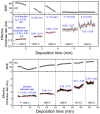
Real-time spectroscopic ellipsometry (RTSE) analysis of (a) Cu and (b) In2Se3 thin films deposited step-wise by evaporation on c-Si substrates at room temperature and at 570 °C, respectively, using five different Cu and In source temperatures, as demarcated by the vertical broken lines. Shown in each top panel is the mean square error (MSE) from the best fit of the RTSE data, and in each bottom panel the instantaneous effective thickness deposition rate Reff = ddeff/dt, which is the instantaneous deposition rate in terms of material volume/area. Average values of the effective thickness deposition rate are included at each source temperature step. For Cu, values of the bulk layer void volume fraction fvb at each temperature step are also included, as deduced from an analysis of the Drude components of the complex dielectric functions ε over the photon energy range of 0.75–1.00 eV.
Figure 4
Figure 4
Deposition rate in terms of effective thickness from the real-time spectroscopic ellipsometry (RTSE) data of Figure 3a,b for (a) Cu and (b) In2Se3, plotted versus the Cu and In evaporation source temperatures, respectively. The RTSE data were collected during the step-wise deposition of five successive layers on a c-Si wafer at room substrate temperature for Cu and at 570 °C for In2Se3. Also shown on the right-hand scale are the Cu and In atom fluxes calculated from the effective thickness rates based on the assumptions of Cu calibration depositions with bulk material void fractions in the 0.112–0.152 range, implicitly included in the effective thickness rates as in Figure 3a, and In2Se3 depositions with single crystal density.
Figure 5
Figure 5
Calibration curves for the settings of the In and Cu source temperatures in CuInSe2 deposition required to obtain specific values of the CIS deposition rate Reff,CIS (horizontal lines) and the [Cu]/[In] composition ratio y (curves). The calibration curves were calculated by applying Equations (4) and (5) using the coefficients dm,n of Table 2 obtained from the Cu and In2Se3 calibration depositions of Figure 4. Experimental results for comparison are included from two series of depositions, one series of CIS films of different y on Mo-coated glass substrates (open squares) and a second series of CIS absorber layer witness samples deposited directly on glass with intended y = 0.90 at different deposition rates Reff,CIS for solar cells (solid circles). Calculations are based on the assumptions of (i) thin film Cu depositions with void fractions of 0.112–0.152, implicitly included in Reff,Cu,Cu as in Figure 3a, and (ii) thicker In2Se3 and CIS depositions having single-crystal density (fv,In2Se3 = fv,CIS = 0).
Figure 6
Figure 6
Measured CIS (a) effective thickness deposition rate Reff,CIS and (b) [Cu]/[In] atomic ratio y plotted as functions of the predicted values for the CIS layers of Figure 5 with 0.87 ≤ y ≤ 0.93. The predicted values are identified based on the two evaporation source temperatures used in the depositions. The deviations between the measurements and predictions can be assigned to variations in the Cu and In atomic concentrations from those assumed in the calibration prediction of Figure 5.
Figure 7
Figure 7
Atomic concentration correction factors fm = 1 − fv,m, where fv,m represents the volume fraction of void, plotted as functions of the evaporation source temperatures for the (a) m = Cu and (b) m = In2Se3 calibration depositions used to develop Figure 8. The factors assigned to Cu are measured relative to Cu, with void fractions in the range 0.112–0.152 implicitly included in the effective thickness rate, as indicated in Figure 3a, and the factors assigned to In are measured relative to In2Se3 of single-crystal density.
Figure 8
Figure 8
Calibration curves for Cu composition ratio y (curves) and CuInSe2 deposition rate Reff,CIS (horizontal lines) for CIS, calculated based on the settings of the In and Cu source temperatures using the Cu and In2Se3 calibration depositions of Figure 3, modified by the atomic concentration corrections of Figure 7. Experimental results for comparison are included from two series of depositions, one series of CIS films of different y (open squares) deposited on Mo-coated glass and a second series at different deposition rates Reff,CIS with intended y = 0.90 as witness samples deposited directly on glass for the absorber layer of solar cells (solid circles). Calibration calculations are based on the assumptions of Cu with void fractions in the range 0.112–0.152, further modified by the corrections in Figure 7a, In2Se3 with material fractions in Figure 7b, and CIS of single-crystal atomic concentrations but with Cu vacancies.
Figure 9
Figure 9
Measured CIS (a) effective thickness deposition rate Reff,CIS and (b) [Cu]/[In] atomic ratio y plotted as functions of the predicted values for the deposited CIS layers of Figure 8 with 0.87 ≤ y ≤ 0.93. The error bar associated with the measured y value is ±0.03. The predicted values are identified according to the two evaporation source temperatures using the atomic concentration corrections of Figure 7. The observed root mean square deviations are reduced compared to those of Figure 6.
Figure 10
Figure 10
(a) X-ray diffraction (XRD) patterns with deduced (b) crystallographic unit cell volumes and (c) crystallite sizes for a series of CIS thin films deposited at different rates with y = 0.90 ± 0.03 at a substrate temperature of 570 °C. These films were deposited on Mo-coated soda-lime glass as co-deposited samples from the rate series of absorber layers in Figure 8 and Figure 9. In (c), Scherrer’s equation was applied independently to the first three XRD peaks representing diffractions from the (112), (220)/(204), and (312)/(116) crystal planes, and an average was also taken (black line). Parts (a,c) are reproduced from [20] with permission, 2021, IEEE PVSC.
Figure 11
Figure 11
Ellipsometry angles (ψ, Δ) measured ex-situ over the photon energy range from 0.74 to 1.25 eV, along with their best fits used to determine the bandgap and Urbach tail slope for two ~2 μm-thick CIS films with measured effective thickness deposition rates of (a) 3.18 Å/s and (b) 6.23 Å/s and y = 0.90 ± 0.03. These samples were deposited on crystalline silicon wafer substrates at a temperature of 570 °C.
Figure 12
Figure 12
(a) Room temperature bandgap deduced from (ψ, Δ) spectra such as those of Figure 11 plotted as a function of effective thickness rate for CIS films with y = 0.90 ± 0.03 deposited on crystalline silicon wafer substrates at 570 °C. (b) The bandgap is also shown as a function of the CIS composition ratio y from mapping SE for a ~600 Å-thick, non-uniform CIS sample deposited at a rate of 7.6 Å/s from Reference [33]. Part (b) is reproduced from [33] with permission, 2018, IEEE WCPEC.
Figure 13
Figure 13
Imaginary parts of the complex dielectric functions ε2 plotted logarithmically versus photon energy for the CIS films deposited at (a) 3.18 Å/s and (b) 6.23 Å/s from the analysis of Figure 11. One ε2 spectrum was obtained by inversion (red squares) using fixed structural parameters, deduced assuming an analytical model for ε2, and another by Kramers–Kronig consistent B-spline smoothing (blue triangles) of the inverted results for ε1 and ε2. Shown are the fits (solid lines) to determine the Urbach tail slopes for the two versions of ε2, as indicated.
Figure 14
Figure 14
(a) Urbach tail slope parameters deduced from the imaginary parts of the dielectric functions ε2 plotted as functions of deposition rate for CIS films with y = 0.90 ± 0.03 deposited at 570 °C. The ε2 spectra were obtained in different ways, including by inversion using fixed structural parameters (red-filled circles) and by B-spline smoothing of the inverted result (black-filled circles), both for films on c-Si wafer substrates. In addition, results obtained from ε2 deduced by through-the-glass SE for CIS films on soda-lime glass substrates are included (open circles). (b) Urbach tail slope parameter as a function of composition ratio y from mapping SE for a 600 Å-thick, non-uniform CIS sample deposited at a rate of 7.6 Å/s from Reference [33]. Part (b) is reproduced from [33] with permission, 2018, IEEE WCPEC.
Figure 15
Figure 15
(a) Relationship between the [Se]/[In] atomic ratio and the [Cu]/[In] atomic ratio for defect models consisting of Cu vacancies without (green line) and with compensating defects (violet line). The compensating defect model 2VCu-InCu is assumed here along with the associated predicted (squares) and observed (triangles) phases [31,32]. Experimental data collected in the present study are also shown for CIS as absorber layers in solar cells (circles). (b) Unit-cell volumes from XRD studies of CIS in the literature [27] and the following ordered defect phases derived from CIS, including Cu3In5Se9 [39], Cu5In9Se16 [39], Cu2In4Se7 [39], Cu3In7Se12 [40], CuIn3Se5 [39], CuIn5Se8 [41,42], and CuIn7Se12 (triangles) [43]. Also shown are corresponding results for a collection of 11 thin-film samples with 0.6 < y < 1.0 (squares) [44].

References

    1. Vossen J.L., Kern W., editors. Thin Film Processes II. Academic; San Diego, CA, USA: 1991.
    1. Smith D.L. Thin-Film Deposition: Principles and Practice. McGraw Hill; New York, NY, USA: 1995.
    1. Mattox D.M. Handbook of Physical Vapor Deposition (PVD) Processing. William Andrew; Norwich, NY, USA: 1998.
    1. Messier R., Troiler-McKinstry S. Thin-film processes. In: Buschow K.H.J., Cahn R.W., Flemings M.C., Ilschner B., Kramer E.J., Mahajan S., Veyssière P., editors. Encyclopedia of Materials: Science and Technology. 2nd ed. Elsevier; Amsterdam, The Netherlands: 2001. pp. 9307–9313.
    1. Thornton J.A. High rate thick film growth. Annu. Rev. Mater. Sci. 1977;7:239–260. doi: 10.1146/annurev.ms.07.080177.001323. - DOI

LinkOut - more resources