

FS-iTFET: advancing tunnel FET technology with Schottky-inductive source and GAA design
- PMID: 39227488
- PMCID: PMC11371965
- DOI: 10.1186/s11671-024-04096-4
FS-iTFET: advancing tunnel FET technology with Schottky-inductive source and GAA design
Abstract
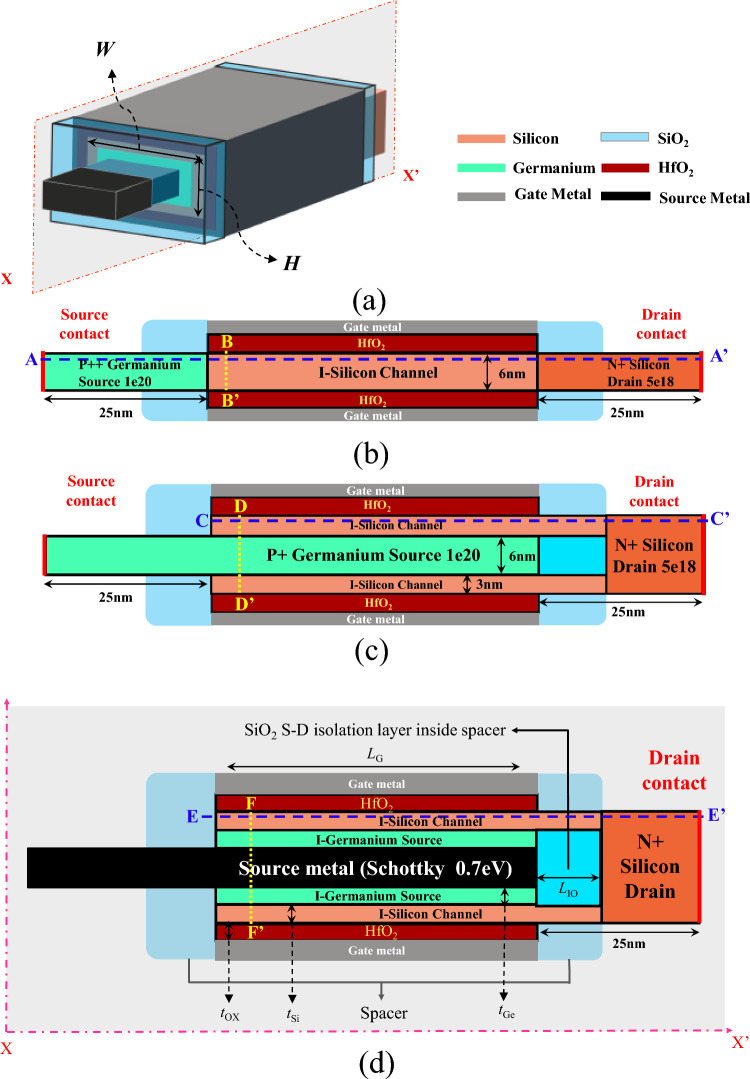
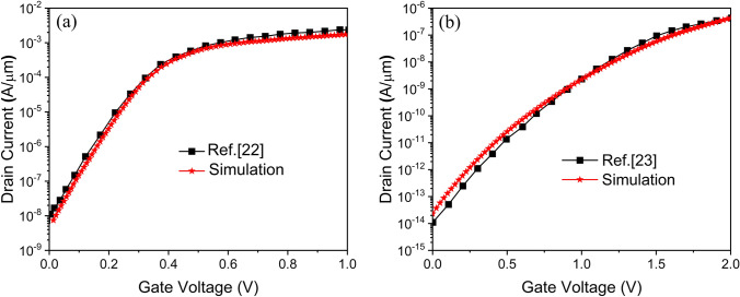
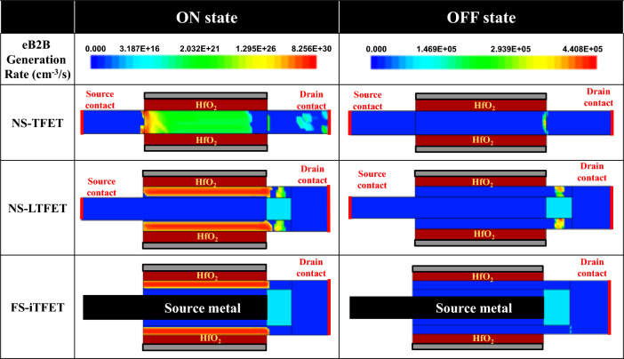
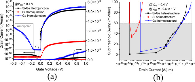
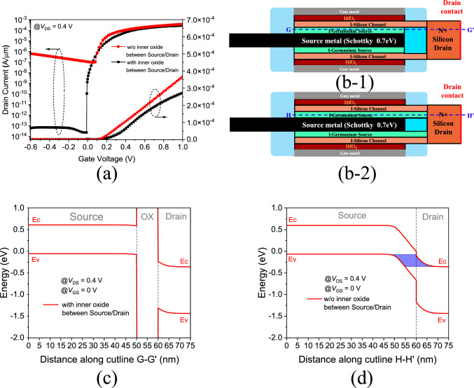
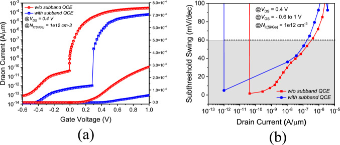
In this paper, we introduce a novel Forkshape nanosheet Inductive Tunnel Field-Effect Transistor (FS-iTFET) featuring a Gate-All-Around structure and a full-line tunneling heterojunction channel. The overlapping gate and source contact regions create a strong and uniform electric field in the channel. Furthermore, the metal-semiconductor Schottky junction in the intrinsic source region induces the required carriers without the need for doping. This innovative design achieves both a steeper subthreshold swing (SS) and a higher ON-state current (ION). Using calibration-based simulations with Sentaurus TCAD, we compare the performance of three newly designed device structures: the conventional Nanosheet Tunnel Field-Effect Transistor (NS-TFET), the Nanosheet Line-tunneling TFET (NS-LTFET), and the proposed FS-iTFET. Simulation results show that, compared to the traditional NS-TFET, the NS-LTFET with its full line-tunneling structure improves the average subthreshold swing (SSAVG) by 19.2%. More significantly, the FS-iTFET, utilizing the Schottky-inductive source, further improves the SSAVG by 49% and achieves a superior ION/IOFF ratio. Additionally, we explore the impact of Trap-Assisted Tunneling on the performance of the three different integrations. The FS-iTFET consistently demonstrates superior performance across various metrics, highlighting its potential in advancing tunnel field-effect transistor technology.
Keywords: Forkshape; Gate ALL around (GAA); Heterojunction; Line tunneling; Metal–semiconductor interface; Nanosheet; Schottky barrier; Subthreshold swing (SS); Tunnel field-effect transistor (TFET).
© 2024. The Author(s).
Conflict of interest statement
The authors declare no competing interests.
Figures


Similar articles
-
Nanosheet integration of induced tunnel field-effect transistor with lower cost and lower power.Discov Nano. 2024 Jul 2;19(1):108. doi: 10.1186/s11671-024-04036-2. Discov Nano. 2024. PMID: 38954140 Free PMC article.
-
Inductive line tunneling FET using epitaxial tunnel layer with Ge-source and charge enhancement insulation.Discov Nano. 2023 Aug 5;18(1):99. doi: 10.1186/s11671-023-03878-6. Discov Nano. 2023. PMID: 37542560 Free PMC article.
-
A novel ultra-steep subthreshold swing iTFET with control gate and control source biasing.Sci Rep. 2025 Aug 2;15(1):28207. doi: 10.1038/s41598-025-13011-5. Sci Rep. 2025. PMID: 40753110 Free PMC article.
-
Enhancing subthreshold slope and ON-current in a simple iTFET with overlapping gate on source-contact, drain Schottky contact, and intrinsic SiGe-pocket.Discov Nano. 2023 Sep 29;18(1):121. doi: 10.1186/s11671-023-03904-7. Discov Nano. 2023. PMID: 37773549 Free PMC article.
-
An Overview of Hot Carrier Degradation on Gate-All-Around Nanosheet Transistors.Micromachines (Basel). 2025 Mar 6;16(3):311. doi: 10.3390/mi16030311. Micromachines (Basel). 2025. PMID: 40141922 Free PMC article. Review.
References
-
- Kumar S, Tiwari P, Zymbler M. Internet of Things is a revolutionary approach for future technology enhancement: a review. J Big Data. 2019;6:111. 10.1186/s40537-019-0268-2.10.1186/s40537-019-0268-2 - DOI
-
- Boucart K, Ionescu AM. Double Gate Tunnel FET with ultrathin silicon body and high-k gate dielectric. In: 2006 European solid-state device research conference. Switzerland: Montreux; 2006. pp. 383–386. 10.1109/ESSDER.2006.307718.
-
- Choi WY, Park B-G, Lee JD, Liu T-JK. Tunneling field-effect transistors (TFETs) with subthreshold swing (SS) less than 60 mV/dec. IEEE Electron Device Lett. 2007;28(8):743–5. 10.1109/LED.2007.901273.10.1109/LED.2007.901273 - DOI
-
- Molaei Imenabadi R, Saremi M, Vandenberghe WG. A novel PNPN-like Z-shaped tunnel field- effect transistor with improved ambipolar behavior and RF performance. IEEE Trans Electron Dev. 2017;64(11):4752–8. 10.1109/TED.2017.2755507.10.1109/TED.2017.2755507 - DOI
Grants and funding
LinkOut - more resources
Full Text Sources
Miscellaneous