Review
. 2024 Sep 4;14(17):1444.
doi: 10.3390/nano14171444.

Single Crystal Sn-Based Halide Perovskites

Affiliations
Review

Single Crystal Sn-Based Halide Perovskites

Aditya Bhardwaj et al. Nanomaterials (Basel). .

Abstract

Sn-based halide perovskites are expected to be the best replacement for toxic lead-based counterparts, owing to their similar ionic radii and the optimal band gap for use in solar cells, as well as their versatile use in light-emitting diodes and photodetection applications. Concerns, however, exist about their stability under ambient conditions, an issue that is exacerbated in polycrystalline films because grain boundaries present large concentrations of defects and act as entrance points for oxygen and water, causing Sn oxidation. A current thriving research area in perovskite materials is the fabrication of perovskite single crystals, promising improved optoelectronic properties due to excellent uniformity, reduced defects, and the absence of grain boundaries. This review summarizes the most recent advances in the fabrication of single crystal Sn-based halide perovskites, with emphasis on synthesis methods, compositional engineering, and formation mechanisms, followed by a discussion of various challenges and appropriate strategies for improving their performance in optoelectronic applications.

Keywords: 2D halide perovskites; Sn perovskites; halide perovskites; lead free; single crystal.


Conflict of interest statement

The authors declare no conflicts of interest.

Figures
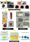
Figure 1
Figure 1
Photographs of the single crystals of Sn-based halide perovskites grown by top-seeded solution growth method: (A) (a) MASnI3 and (b) FASnI3 by optimization of growth conditions (reproduced with permission [26], Copyright Wiley). (B) (a–e) Pb-Sn mixed-halide MAPbxSn1−xBr3 (MA-CH3NH3) single crystals (reproduced with permission [27], Copyright, ACS Publications), hydrothermal method: (C) Color changes of Cs2SnCl6−xBrx from transparent to yellow to red (reproduced with permission [28], Copyright Wiley). (D) Bridgman method for the growth of mixed-halide perovskite single crystals of Cs(Pb0.75Sn0.25)(Br1.00Cl2.00) (a) ingot after crystal growth, (b) polished crystal from cleaved part of the ingot (reproduced with permission [31], Copyright Springer Nature. (E) Inverse temperature crystallization for the growth of mixed-halides (MAPbI3)x(FASnI3)1−x (x is 0.8, 0.5, 0.2) (reproduced with permission [34], Copyright ACS Publications). (F) Space-confined method for the growth of mixed-halide (FASnI3)0.1(MAPbI3)0.9 perovskites (reproduced with permission [36], Copyright Royal Society of Chemistry).
Figure 2
Figure 2
(A) Reductant engineering method using oxalic acid for the growth of FPEA2SnI4 single crystals (reproduced with permission [37], Copyright Wiley). (B) Ethylene glycol and HI-assisted modified temperature lowering method for fabrication of 2D (4-FPEA)2SnI4 tin halide perovskite single crystals (reproduced with permission [38], Copyright ACS Publications). (C) Synthesis process for fabrication of 1D perovskite single crystal-MDASn2I6 and its corresponding image and dimensions (reproduced with permission [49], Copyright ACS Publications). (D) Single crystals of (a) (R/S-α-PEA)SnCl3 and (b) (R/S-α-PEA)SnBr3 of sizes-6 mm, 10 mm by bottom seeded solution growth (reproduced with permission [50], Copyright Wiley). (E) Single crystals of B-γ CsSnI3 by solvent volatilization method (reproduced with permission [51], Copyright Royal Society of Chemistry).
Figure 3
Figure 3
(A,B) Energy band structures and DOS of CsSnCl3, CsSnBr3, CsSnI3 (reproduced with permission [55], Copyright MDPI). (C) Band-bowing in mixed-halide perovskites of MA(Pb1−xSnx)I3 (reproduced with permission [57], Copyright ACS). (D) Partial density of states of p-orbital electron in MASnaPb1-aI3 mixed-halide perovskites (a-0, 0.25, 0.5, 0.75, 1) (reproduced with permission [58], Copyright Elsevier).
Figure 4
Figure 4
(A) Calculated defect formation energies in CsSnI3 as a function of the chemical potentials of electrons, Cs, and Sn. Points A and E correspond to Sn-rich growth conditions, while points B, C, and E correspond to Sn-poor growth conditions. Empty (solid) circles represent acceptor (donor) defects. (B) Calculated transition energies for various defects, with acceptor (donor) defect levels shown in red (blue). The number of empty (solid) circles denotes the number of holes (electrons) released following defect ionization. (Reproduced with permission [66], Copyright ACS).
Figure 5
Figure 5
(A) (a) Schematic of Cs2SnCl6−xBrx single crystal photodetector device, (b) mechanism of the photodetector, where Ip, Ie, ID denote penetration, electron diffusion, and drift length; (c) current vs. time response at −20 V bias with illumination wavelengths of 590, 610, and 560 nm with light intensity of 1.3 mW/cm2 (reproduced with permission [28], Copyright Wiley). (B) (a–c) current vs. time response of (MAPbI3)x(FASnI3)1−x (x = 0.8, 0.5, and 0.2) single crystals at 0 V bias with channel width of 30, 50, and 100 m in wavelength range of 405–1064 nm with light intensity of 0.60 mW/cm2 (reproduced with permission [34], Copyright ACS). (C) Device structure of 2D Cs2SnI6 single crystals and current vs. time response at different power densities at 1 V bias under illumination by light of wavelength 405 nm (reproduced with permission [72], Copyright Elsevier). (D) (a–c) current vs. voltage curves of (C8H9F3N)2Pb1−xSnxI4 (x = 0, 0.5, and 1) single-crystal photodetectors, where the insets depict the device structure and optical microscope images in dark and illumination with light of wavelengths 405, 650 nm with light intensity of 0.006, 6.37, and 70.7 mW/mm2. The current vs. time curves were obtained at 5, 10 V bias (reproduced with permission [25], Copyright Royal Society of Chemistry).
Figure 6
Figure 6
(A) (a) Cross-section scanning electron microscope image of C-CsSnI3, (b) photocurrent density vs. voltage curve, (c) stabilized power output, and (d) external quantum efficiency curves of C-CsSnI3, S-CsSnI3 perovskite solar cells (reproduced with permission [51], Copyright Royal Society of Chemistry). (B,C) Mobility-lifetime values, sensitivity, of X-ray detectors of FPEA2PbI4 and heterojunction FPEA2PbI4-FPEA2SnI4 tin single crystal, X-ray photocurrent signals, operational stability of FPEA2PbI4-FPEA2SnI4 (reproduced with permission [37], Copyright Wiley). (D) (a,d) Microphotoluminescence spectra, (b,e) FWHM, integrated intensity of emission peaks as function of pump density, (c,f) time-resolved photoluminescence spectra below and above pump fluence threshold of (TEA)2SnI4 and (TEA)2(MA)Sn2I7 tin perovskite single crystals (reproduced with permission [42], Copyright Royal Society of Chemistry). (E) (a) FET device structure, (b) transfer curve, (c) current vs. voltage curve, (d) on–off switching curves showing good stability of 4AMPSnI4 Dion–Jacobson tin perovskite single crystals (Reproduced with permission [43], Copyright ACS).

Similar articles

Cited by

References

    1. Zhou D., Zhou T., Tian Y., Zhu X., Tu Y. Perovskite-Based Solar Cells: Materials, Methods, and Future Perspectives. J. Nanomater. 2018;2018:8148072. doi: 10.1155/2018/8148072. - DOI
    1. Jellicoe T.C., Richter J.M., Glass H.F.J., Tabachnyk M., Brady R., Dutton S.E., Rao A., Friend R.H., Credgington D., Greenham N.C., et al. Synthesis and Optical Properties of Lead-Free Cesium Tin Halide Perovskite Nanocrystals. J. Am. Chem. Soc. 2016;138:2941–2944. doi: 10.1021/jacs.5b13470. - DOI - PubMed
    1. Jiang X., Zang Z., Zhou Y., Li H., Wei Q., Ning Z. Tin Halide Perovskite Solar Cells: An Emerging Thin-Film Photovoltaic Technology. Acc. Mater. Res. 2021;2:210–219. doi: 10.1021/accountsmr.0c00111. - DOI
    1. Abate A. Perovskite Solar Cells Go Lead Free. Joule. 2017;1:659–664. doi: 10.1016/j.joule.2017.09.007. - DOI
    1. Abate A. Stable Tin-Based Perovskite Solar Cells. ACS Energy Lett. 2023;8:1896–1899. doi: 10.1021/acsenergylett.3c00282. - DOI - PMC - PubMed

LinkOut - more resources