Growth of Single Crystals of (K1-xNax)NbO3 by the Self-Flux Method and Characterization of Their Phase Transitions
- PMID: 39274588
- PMCID: PMC11396741
- DOI: 10.3390/ma17174195
Growth of Single Crystals of (K1-xNax)NbO3 by the Self-Flux Method and Characterization of Their Phase Transitions
Abstract
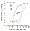
In this study, single crystals of (K1-xNax)NbO3 are grown by the self-flux crystal growth method and their phase transitions are studied using a combination of Raman scattering and impedance spectroscopy. X-ray diffraction shows that single crystals have a perovskite structure with monoclinic symmetry. Single crystal X-ray diffraction shows that single crystals have monoclinic symmetry at room temperature with space group P1211. Electron probe microanalysis shows that single crystals are Na-rich and A-site deficient. Temperature-controlled Raman scattering shows that low temperature monoclinic-monoclinic, monoclinic-tetragonal and tetragonal-cubic phase transitions take place at -20 °C, 220 °C and 440 °C. Dielectric property measurements show that single crystals behave as a normal ferroelectric material. Relative or inverse relative permittivity peaks at ~-10 °C, ~230 °C and ~450 °C with hysteresis correspond to the low temperature monoclinic-monoclinic, monoclinic-tetragonal and tetragonal-cubic phase transitions, respectively, consistent with the Raman scattering results. A conduction mechanism with activation energies of about 0.5-0.7 eV was found in the paraelectric phase. Single crystals show polarization-electric field hysteresis loops of a lossy normal ferroelectric. The combination of Raman scattering and impedance spectroscopy is effective in determining the phase transition temperatures of (K1-xNax)NbO3.
Keywords: (K0.5Na0.5)NbO3; Raman scattering; impedance spectroscopy; lead-free piezoelectric; self-flux crystal growth; single crystal.
Conflict of interest statement
The authors declare no conflicts of interest.
Figures


References
-
- Rödel J., Jo W., Seifert K.T.P., Anton E.M., Granzow T., Damjanovic D. Perspective on the Development of Lead-free Piezoceramics. J. Am. Ceram. Soc. 2009;92:1153–1177. doi: 10.1111/j.1551-2916.2009.03061.x. - DOI
-
- Gupta S., Maurya D., Yan Y., Priya S. Development of KNN-Based Piezoelectric Materials. In: Priya S., Nahm S., editors. Lead-Free Piezoelectrics. Springer; New York, NY, USA: 2012. pp. 89–119.
-
- Safari A., Hejazi M. Lead-Free KNN-Based Piezoelectric Materials. In: Priya S., Nahm S., editors. Lead-Free Piezoelectrics. Springer; New York, NY, USA: 2012. pp. 139–175.
-
- Wu J. Advances in Lead-Free Piezoelectric Materials. Springer Nature; Singapore: 2018.
-
- Zheng T., Wu J., Xiao D., Zhu J. Recent development in lead-free perovskite piezoelectric bulk materials. Prog. Mater. Sci. 2018;98:552–624. doi: 10.1016/j.pmatsci.2018.06.002. - DOI
Grants and funding
LinkOut - more resources
Full Text Sources

