. 2024 Sep 24;121(39):e2408974121.
doi: 10.1073/pnas.2408974121. Epub 2024 Sep 18.

Atomic-engineered gradient tunable solid-state metamaterials

Affiliations

Atomic-engineered gradient tunable solid-state metamaterials

Zhiyuan Yan et al. Proc Natl Acad Sci U S A. .

Abstract

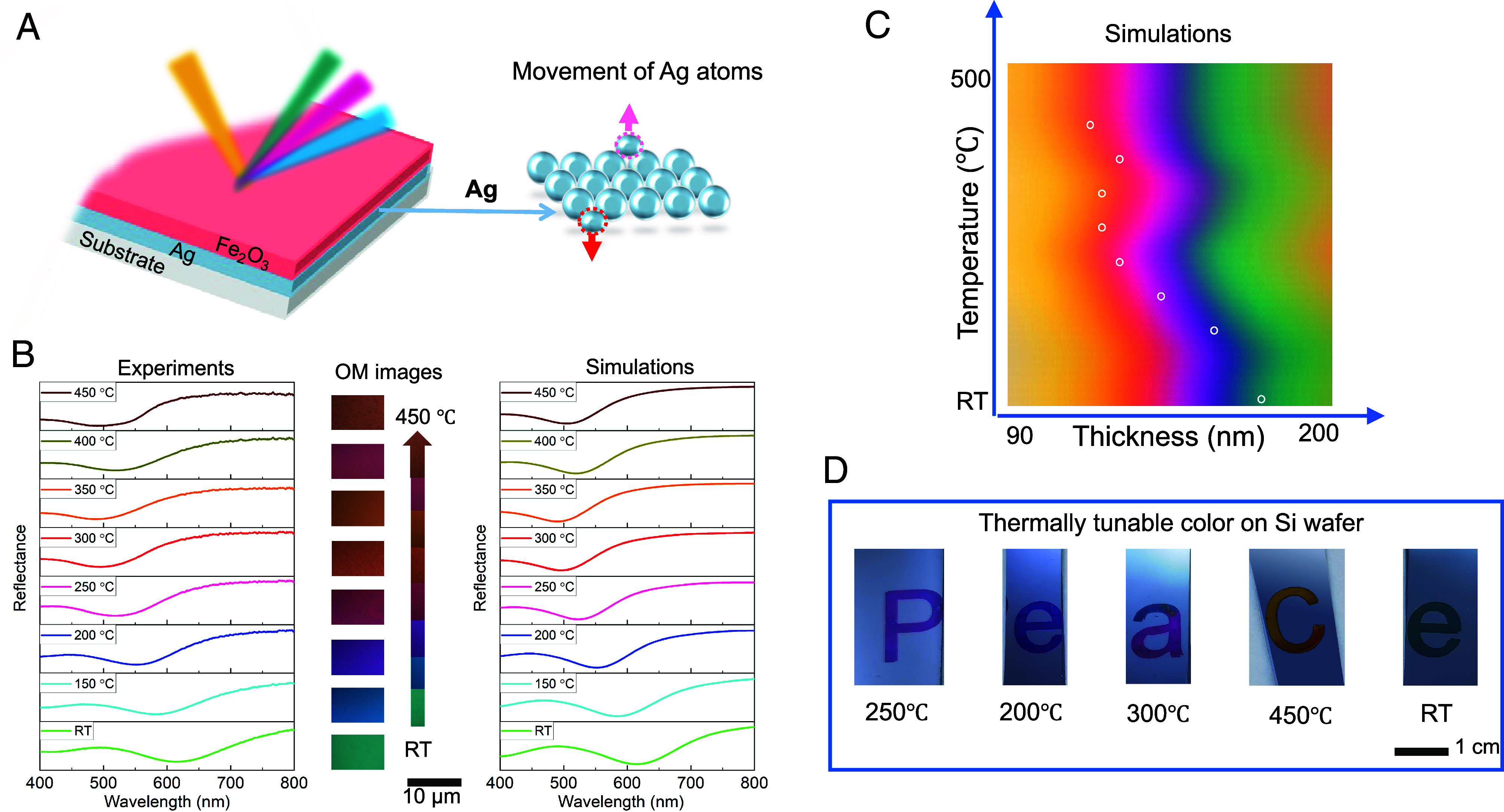
Metamaterial has been captivated a popular notion, offering photonic functionalities beyond the capabilities of natural materials. Its desirable functionality primarily relies on well-controlled conditions such as structural resonance, dispersion, geometry, filling fraction, external actuation, etc. However, its fundamental building blocks-meta-atoms-still rely on naturally occurring substances. Here, we propose and validate the concept of gradient and reversible atomic-engineered metamaterials (GRAM), which represents a platform for continuously tunable solid metaphotonics by atomic manipulation. GRAM consists of an atomic heterogenous interface of amorphous host and noble metals at the bottom, and the top interface was designed to facilitate the reversible movement of foreign atoms. Continuous and reversible changes in GRAM's refractive index and atomic structures are observed in the presence of a thermal field. We achieve multiple optical states of GRAM at varying temperature and time and demonstrate GRAM-based tunable nanophotonic devices in the visible spectrum. Further, high-efficiency and programmable laser raster-scanning patterns can be locally controlled by adjusting power and speed, without any mask-assisted or complex nanofabrication. Our approach casts a distinct, multilevel, and reversible postfabrication recipe to modify a solid material's properties at the atomic scale, opening avenues for optical materials engineering, information storage, display, and encryption, as well as advanced thermal optics and photonics.

Keywords: atomic manipulation; heterogeneous interface; metaoptics; phase transition.


Conflict of interest statement

Competing interests statement:The authors declare no competing interest.

Figures

Fig. 1.
Fig. 1.
GRAM concept and atomic manipulation strategy. (A and B) A schematic comparison highlights the limitations of conventional methods (limited tunability) versus the versatility of our approach. Dynamic refractive index changes are represented by colors, while volume alterations are depicted by shape variations. (C) The working principle of gradient and reversible atomic manipulation is demonstrated: the amorphous host with a heterogeneous interface (i) Gradient movement in amorphous host (ii and iii) “Backhaul of metal atoms” during phase transition from amorphous to crystal in the host (iv). Inset figures reveal the displacement of noble metal atoms under a thermal field, characterized by the initial temperature (To) and real-time temperature (Tt).
Fig. 2.
Fig. 2.
GRAM powered through the heterogeneous interface and mechanism of the nonbinary metamaterials. (AC) Schematic illustrations of the differences among the current mechanism of volatile atomic mobility in crystals (A) unidirectional nonvolatile atomic mobility in amorphous host (B) and our proposed GRAM (C): (A) Crystalline host/metal with stagnant interface; (B) amorphous host/metal with metal trapping and overflow; (C) amorphous host with a top heterogeneous interface enabling controllable gradient and reversible metal atoms movement. (DG) Experimental characterization showing gradient moving of noble metal atoms in amorphous host: (D) TEM images displaying the vertical architecture of the metaphotonic device on Si substrate after annealing at 200 °C for 1 min. (E and F) EDX mapping and line profile of three key elements (Fe, Ag, and O). (Scale bar: 100 nm.) (G) XRD results showing the amorphous states of host annealing at 200 °C. (HK) Experimental characterization showing reversible moving of noble metal atoms assisted by phase transition of host: (H) TEM images of the vertical architecture of the same device annealed at 500 °C for 1 min. (I and J) EDX mapping and line profile of three key elements (Fe, Ag, and O). (Scale bar: 100 nm.) (K) XRD characterization showing the crystalline state of host after annealing at 500 °C.
Fig. 3.
Fig. 3.
Phase transition of amorphous host. (AD) MD simulations of the phase transition of the amorphous host induced by a top atom heterogeneous interface of amorphous Fe2O3: (A) initial amorphous state with a top crystalline heterogeneous interface. (BD) Crystallization process of amorphous Fe2O3 for 3 ns at 800 K. (EK) X-ray absorption fine structure (XAFS) spectra of the dynamic phase transition process. (E and F) Comparative XANES features for peaks A and B, contrasting as-deposited (RT) devices with those annealed at temperatures ranging from 150 to 250 °C (E) and 350 to 450 °C (F). (G and H) XANES spectra for peak B, juxtaposing the RT and annealed samples within the 150 to 250 °C (G) and 350 to 450 °C (H) intervals. (I) XANES spectral comparison among the RT sample, the one annealed at 500 °C, and the reference α-Fe2O3. (J) K2-weighted Fourier transformed EXAFS analysis comparing the RT device, those annealed from 150 to 500 °C, and the standard α-Fe2O3. (K) First-shell fitting of the non-phase-shift-corrected Fourier transform for the Fe K-edge of the sample annealed at 450 °C, with black and blue indicating experimental results, and red and orange representing calculated results.
Fig. 4.
Fig. 4.
Proof-of-concept demonstration of nonbinary solid metaphotonics for large-scale color printing. (A) Schematic representation of the adjustable optical instrument utilizing the GRAM concept. (B) On the Left, observed reflectance and on the Right, computed spectral data for a specimen subjected to various annealing temperatures (ranging from 150 to 450 °C), with OM imagery in natural lighting for each specific temperature. The images include a scale marker of 10 µm. (C) Color mapping simulations conducted in conjunction with Ag atom adjustments, displaying a gradient of color points from room temperature to 450 °C, arranged from the Lower Right to the Upper Left. (D) The process of color imprinting and thermally induced color modulation of the word “Peace” on a Si substrate, with photographic evidence of each character exhibiting a spectrum of colors at varying temperatures, denoted by a scale marker of 1 cm.
Fig. 5.
Fig. 5.
One-step pattern generation by local laser actuation. (A) Schematic illustration of the gradient and reversible color-pattern generation on a Si wafer using a high-efficiency laser, without complex lithography process. (B) OM images of the raster-scanning pattern with different laser powers from 1 to 75 mW and a fixed speed of 1 μm/ms. (C) OM images of the programmable reversible color pattern with different laser powers from 10 to 75 mW and a fixed speed of 0.3 μm/ms. (D) Large-scale Butterfly demonstration on Si wafer in 10 s with a laser power of 10 mW. (E) RGB color Flower patterns generated by local laser raster-scanning with programmed power. (F) Reversible generation of high-resolution patterns by the GRAM mechanism. The color patterns inspired by Composition avec blue, rouge, jaune et noir.

References

    1. Zheludev N. I., Kivshar Y. S., From metamaterials to metadevices. Nat. Mater. 11, 917–924 (2012). - PubMed
    1. Liu Y., Zhang X., Metamaterials: A new frontier of science and technology. Chem. Soc. Rev. 40, 2494–2507 (2011). - PubMed
    1. Sihvola A., Metamaterials in electromagnetics. Metamaterials 1, 2–11 (2007).
    1. Liu Y., et al. , Dynamic thermal camouflage via a liquid-crystal-based radiative metasurface. Nanophotonics 9, 855–863 (2020).
    1. Tittl A., et al. , Imaging-based molecular barcoding with pixelated dielectric metasurfaces. Science 360, 1105–1109 (2018). - PubMed

LinkOut - more resources