. 2024 Sep 20;10(38):eado4142.
doi: 10.1126/sciadv.ado4142. Epub 2024 Sep 18.

Two-dimensional silk

Affiliations

Two-dimensional silk

Chenyang Shi et al. Sci Adv. .

Abstract

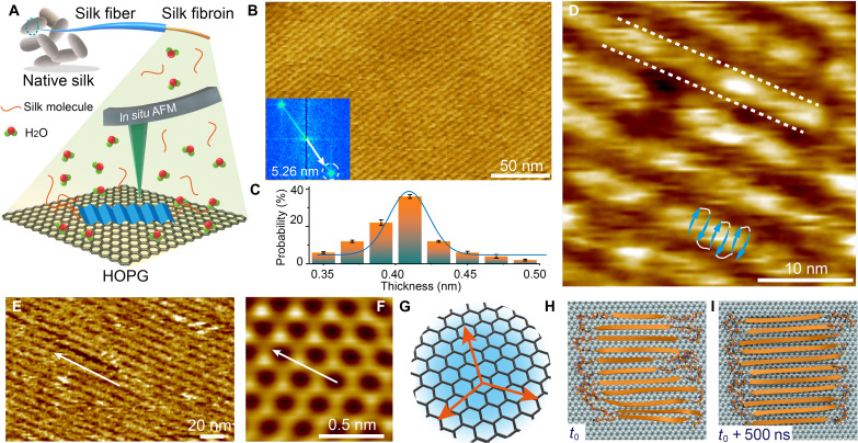
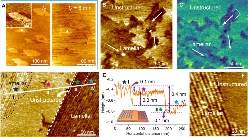
Despite the promise of silk-based devices, the inherent disorder of native silk limits performance. Here, we report highly ordered two-dimensional silk fibroin (SF) films grown epitaxially on van der Waals (vdW) substrates. Using atomic force microscopy, nano-Fourier transform infrared spectroscopy, and molecular dynamics, we show that the films consist of lamellae of SF molecules that exhibit the same secondary structure as the nanocrystallites of native silk. Increasing the SF concentration results in multilayers that grow either by direct assembly of SF molecules into the lamellae or, at high concentrations, along a two-step pathway beginning with a disordered monolayer that then crystallizes. Scanning Kelvin probe measurements show that these films substantially alter the surface potential; thus, they provide a platform for silk-based electronics on vdW solids.


Figures

Fig. 1.
Fig. 1.. The structure of 2D SF lamellae grown epitaxially on HOPG.
(A) Scheme of SF assembly on HOPG characterized by in situ AFM. (B) AFM image of a lamellar SF monolayer on HOPG formed at an SF concentration of 0.05 μg/ml and an incubation time of 30 min. Inset shows corresponding fast Fourier transform (FFT) pattern. (C) Thickness distribution of the lamellae. (D) AFM image of SF lamellae showing distinct segments. The illustration consisting of solid blue arrows and white connectors indicates how the antiparallel array of individual SF β strands from the MD simulations maps onto the lamellae and is not intended to be dimensionally accurate. The blue arrows correspond the orange arrows in (H). Dashed white lines delineate the boundary of single lamellae. The SF concentration is 0.05 μg/ml, and the incubation time is 60 min. (E and F) AFM images of (E) SF lamellar structure and (F) underlying HOPG lattice showing that lamellae lie along the armchair lattice direction as illustrated in (G). The SF concentration is 0.05 μg/ml, and the incubation time is 30 min. (H and I) Simulations of SF β sheet binding to HOPG. An SF protein with β sheet conformation initially aligned along the armchair direction (H) remains structured in that alignment after 500 ns (I). To determine the geometric relationship between the SF lamellae and the underlying HOPG lattice structure (F), the SF film (E) was scratched off using contact mode AFM in liquid.
Fig. 2.
Fig. 2.. The structure of SF multilayers.
(A and B) Two consecutive AFM images of multilayer SF lamellae. The SF concentration is 0.1 μg/ml, and the incubation time t0 is about 70 min. The inset in (A) shows the corresponding FFT pattern. White arrows indicate the three directions of the lamellae. The white dashed boundaries delineate two domains (i and ii) of lamellae overlaying the lower layer. The inset in (B) illustrates the two possible stacking configurations, coaligned and at 120° angles. (C) In situ AFM phase images of lamevvvllae, showing the replacement of a crossed domain by a coaligned domain. The white arrows indicate the orientation within and outside of the crossed domain, which is delineated by the white dashed boundaries. The SF concentration is 0.1 μg/ml, and the incubation time t0 is about 90 min. (D and E) MD simulations of bilayer SF lamellae with (D) face-to-face and (E) front-to-back packing. (F) Color map showing the time evolution of the in situ nano-FTIR spectra during SF assembly on graphene from an aqueous SF solution of 0.1 μg/ml. (G) In situ nano-FTIR spectra of SF lamellae and ex situ attenuated total reflection (ATR)–FTIR spectrum of dehydrated SF bulk material (see the section “In situ nano-FTIR characterization” in Materials and Methods for details). The insets illustrate the amide I and II vibration modes during IR absorption (left) and the expected vibration mode of the ordered amide group on graphene (right), both from the MD simulations of the SF configuration within the lamellae and the lack of an amide I signal in the nano-FTIR spectra.
Fig. 3.
Fig. 3.. The two-step growth process of lamellar SF films.
(A) Consecutive AFM height images of an unstructured film forming from SF solution (0.2 μg/ml). The inset shows that the unstructured film is deposited on a lamellar layer. The incubation time is 20 min. (B and C) AFM height (B) and phase images (C) during SF assembly from SF solution (1 μg/ml). The incubation time is 25 min. White arrows indicate the three directions of the lamellae. Both lamellar and unstructured domains can be easily identified in both, indicating that the domains differ in stiffness. (D) AFM height image showing two complete layers in which lamellar and unstructured regions coexist. The white dashed line delineates the edge of the upper layer. The black dashed boundary denotes a lamellar region in the upper layer, while the white dashed boundary denotes an unstructured region in the lower layer. The SF concentration is 0.2 μg/ml, and the incubation time is 57 min. (E) Height profile along the solid white line in (D). Blue, pink, green, and cyan stars denote different structural regions: lamellar (blue and cyan) and unstructured (pink and green). The inset illustrates the model of multilayer SF films with ordered and disordered regions. (F) High-magnification AFM height image of the boundary between lamellar and unstructured domains. The SF concentration is 0.2 μg/ml, and the incubation time is 65 min.
Fig. 4.
Fig. 4.. The phase transition process of lamellar SF films.
(A to C) Consecutive AFM images of assembly from SF solution (1 μg/ml) showing the phase transition from unstructured to lamellar. The incubation time is 50 min. The white dashed lines mark the boundaries between the two. (D) Proposed model for the two-step process of the lamellar SF film formation. (E) In situ nano-FTIR spectra showing the change in secondary structure during assembly on graphene in high-concentration SF solution (0.5 μg/ml), along with an illustration of the process. (F) Corresponding color map intensity of the nano-FTIR spectra as a function of time.
Fig. 5.
Fig. 5.. The mechanism of 2D SF assembly at the water-HOPG interface.
(A) Depiction of bulk SF fibrils structure at mesoscopic and macroscopic scales. (B to H) Proposed scheme of 2D SF assembly at the water-HOPG interface. (I and J) AFM height image (I) and corresponding SKPM image (J) showing that the top SF film was selectively removed from the bright region in (J) through scraping to reveal the underlying HOPG where the surface potential is significantly higher. (K and L) AFM height image (K) and corresponding SKPM image (L) of SF film on HOPG.

References

    1. Good I. L., Kenoyer J. M., Meadow R. H., New evidence for early silk in the Indus civilization. Archaeometry 51, 457–466 (2009).
    1. Kim S., Marelli B., Brenckle M. A., Mitropoulos A. N., Gil E.-S., Tsioris K., Tao H., Kaplan D. L., Omenetto F. G., All-water-based electron-beam lithography using silk as a resist. Nat. Nanotechnol. 9, 306–310 (2014). - PubMed
    1. Huang W., Ling S., Li C., Omenetto F. G., Kaplan D. L., Silkworm silk-based materials and devices generated using bio-nanotechnology. Chem. Soc. Rev. 47, 6486–6504 (2018). - PMC - PubMed
    1. Shi C., Hu F., Wu R., Xu Z., Shao G., Yu R., Liu X. Y., New silk road: From mesoscopic reconstruction/functionalization to flexible meso-electronics/photonics based on cocoon silk materials. Adv. Mater. 33, e2005910 (2021). - PubMed
    1. Shi C., Wang J., Sushko M. L., Qiu W., Yan X., Liu X. Y., Silk flexible electronics: From Bombyx mori silk Ag nanoclusters hybrid materials to mesoscopic memristors and synaptic emulators. Adv. Funct. Mater. 29, 1904777 (2019).