. 2024 Oct;634(8032):74-79.
doi: 10.1038/s41586-024-07941-9. Epub 2024 Sep 18.

Advanced CMOS manufacturing of superconducting qubits on 300 mm wafers

Affiliations

Advanced CMOS manufacturing of superconducting qubits on 300 mm wafers

J Van Damme et al. Nature. 2024 Oct.

Abstract

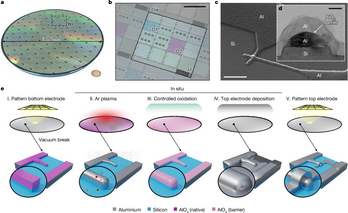
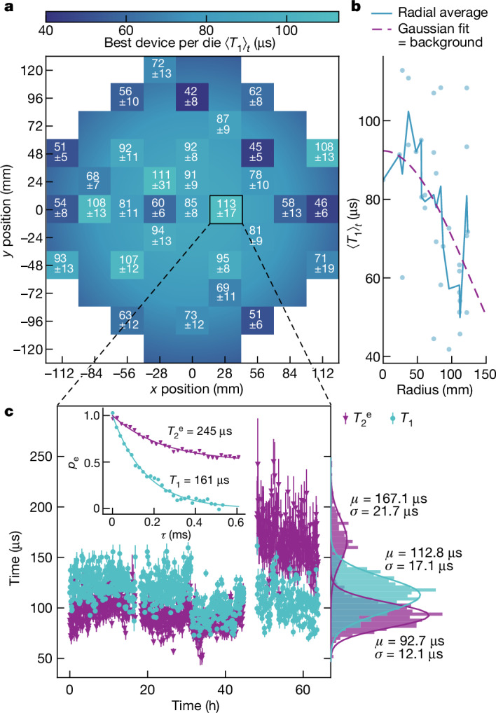
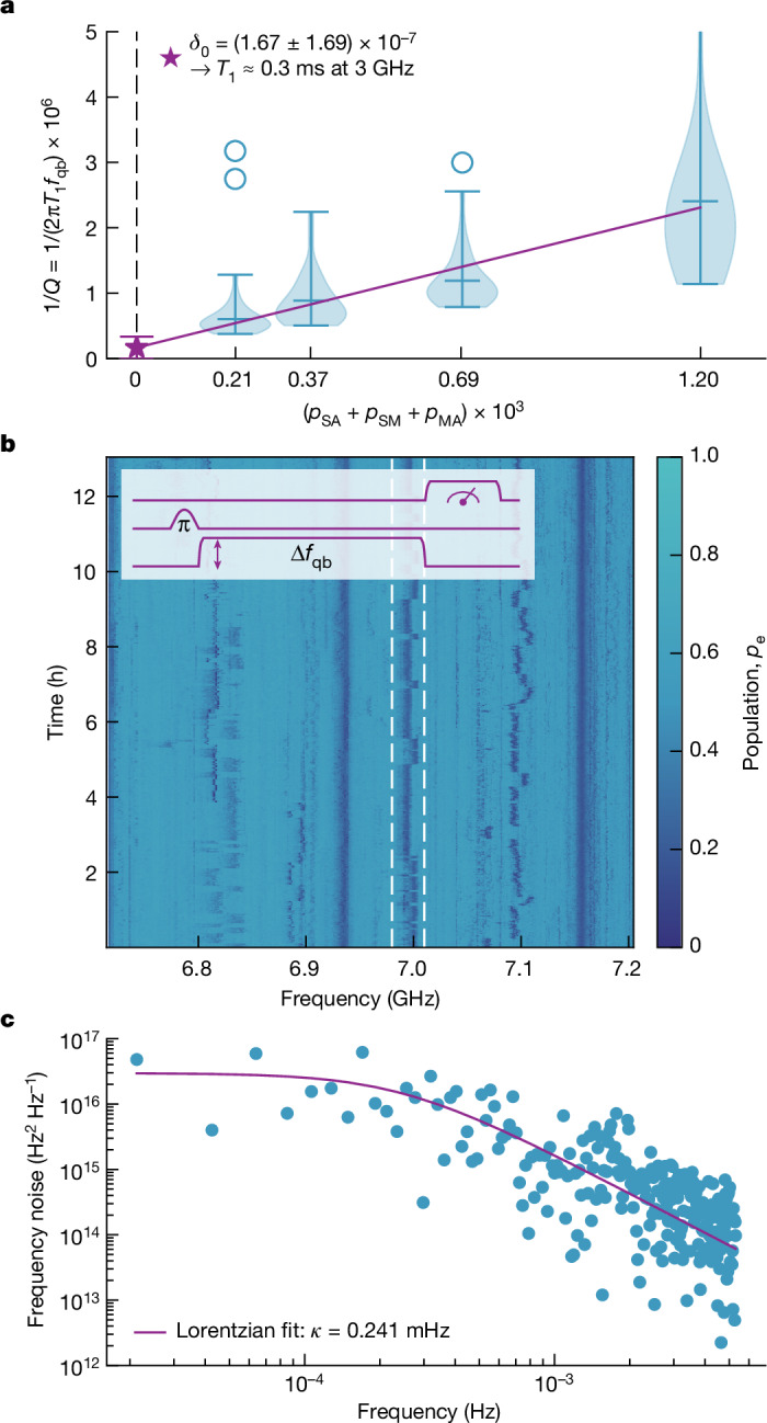
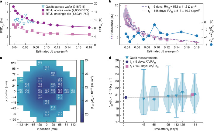
The development of superconducting qubit technology has shown great potential for the construction of practical quantum computers1,2. As the complexity of quantum processors continues to grow, the need for stringent fabrication tolerances becomes increasingly critical3. Utilizing advanced industrial fabrication processes could facilitate the necessary level of fabrication control to support the continued scaling of quantum processors. However, at present, these industrial processes are not optimized to produce high-coherence devices, nor are they a priori compatible with the approaches commonly used to make superconducting qubits. Here we demonstrate superconducting transmon qubits manufactured in a 300 mm complementary metal-oxide-semiconductor (CMOS) pilot line using industrial fabrication methods, with resulting relaxation and coherence times exceeding 100 μs. We show across-wafer, large-scale statistics of coherence, yield, variability and ageing that confirm the validity of our approach. The presented industry-scale fabrication process, which uses only optical lithography and reactive-ion etching, has a performance and yield in line with conventional laboratory-style techniques utilizing metal lift-off, angled evaporation and electron-beam writing4. Moreover, it offers the potential for further upscaling through three-dimensional integration5 and more process optimization. This result marks the advent of an alternative and new, large-scale, truly CMOS-compatible fabrication method for superconducting quantum computing processors.


Conflict of interest statement

The authors declare no competing interests.

Figures

Fig. 1
Fig. 1. Fabrication of overlap JJ qubit.
a, Photograph of the 300 mm wafer. b, Photograph of one die with subdie designs D1 and D2 highlighted. c, SEM image of an overlap JJ. d, Transmission electron microscopy image of a cross section of the junction (dashed line in c). e, Schematic representation of the key fabrication steps for an overlap JJ. Scale bars, 10 mm (b), 1 μm (c), 50 nm (d).
Fig. 2
Fig. 2. Qubit relaxation and coherence times.
a, Wafer map of time-averaged relaxation times T1t of the best-performing qubit on each measured die. The mean values and standard deviations are printed at each measured location. b, The background colour (a) represents a heuristic Gaussian fit to the average value as a function of radius. c, Repeated measurements of the relaxation time T1 and Hahn-echo coherence time T2e of the best-performing qubit on die (1,0) over 60 h. The time statistics are represented by histograms with Gaussian fits of mean µ and standard deviation σ. Inset, example traces of the relaxation and decoherence of the qubit excited state population (pe) as a function of delay time (τ).
Fig. 3
Fig. 3. Interface TLS defects.
a, Qubit loss (1/Q-factor) as a function of the total interface participation ratio (substrate–air, metal–air and substrate–metal) of the electric field energy for four different qubit designs on subdies D1 across the wafer. The distributions of each design were filtered for outliers beyond the interquartile range and visualized with violin plots including the mean and extrema (outliers shown as scatter points). The linear fit extrapolates the loss to zero interface participation and extracts the upper bound on the relaxation time. b, A flux-tunable qubit population as a function of qubit frequency measured repeatedly over 13 h to visualize the dynamics of relaxation channels associated with TLS defects at interfaces. Inset, the pulse sequence used to scan the spectrum. c, Frequency noise power spectral density of the highlighted defect in b, including Lorentzian fit with full-width at half-maximum linewidth κ.
Fig. 4
Fig. 4. Qubit frequency variability and ageing analysis.
a, RSDs of qubit frequencies and normal state resistances of JJ test structures (RSDfqb=RSDRn/2, visualized with the double y axes) as a function of the estimated JJ area. 9 (qubits per die) × 24 (dies) = 216 qubits across the wafer, 8 (JJs per area per die) × 12 (areas) × 82 (dies) = 7,872 JJs across a wafer, 146 (JJs per area) × 12 (areas) = 1,752 JJs on a die (0,2). All working qubits are included. The resistances of JJ test structures were filtered per area for outliers beyond 1.5 times the interquartile range. Solid lines are fits to equation (2). b, Normal resistances of JJ test structures as a function of estimated junction area for a subgroup of 216 devices measured 5 days after fabrication (t0) and once more 146 days after fabrication. The right y axis shows the corresponding change in the relative average resistance for each JJ area. c, Wafer map of qubit frequencies scaled with A (where A is the estimated JJ area) and ensemble averaged (⟨⟩e) over the nine qubits on each subdie D2. The mean values are accompanied by the standard deviation. The background colour represents a heuristic Gaussian fit to the average value as a function of radius. d, Area-scaled qubit frequencies of qubits on subdies D2 plotted as a function of cool-down time after fabrication, compared with the product of the resistance and area of the JJs extracted from the fits in b scaled with a proportionality factor XΔEC/he2 (where Δ is the superconducting gap of aluminium, EC is the qubit charging energy, h is Planck’s constant and e is the elementary charge). The black vertical dashed line represents the wafer fabrication date at t0. Distributions of measured qubits are represented by violin plots showing means and extrema. The grey area indicates the ageing from JJ data.
Extended Data Fig. 1
Extended Data Fig. 1. Two-level system counting.
a, Time-frequency map (main text Fig. 3b) with highlighted two-level systems. b, Example slice of a illustrating the detected TLS at one timestamp.
Extended Data Fig. 2
Extended Data Fig. 2. JJ area estimation.
a, SEM image of a JJ after BE patterning. b, SEM image of a JJ after TE patterning. c, TEM image of a cross section of a JJ, including an ellipse circumference as approximation of the rounded BE surface. d, Average width of the JJ’s BE and TE measured from the SEM images a,b. The solid lines are linear fits including a constant offset. e, Best effort estimate of the JJ area, calculated for each designed JJ critical dimension.
Extended Data Fig. 3
Extended Data Fig. 3. Resistance variance area dependence model comparison.
a, Relative standard deviation of JJ normal resistances measured across the wafer and on a single die as function of the estimated JJ area (same data as Fig. 4a). The solid lines represent the best fit with model A of constant area variance (A/dA = 0), the dashed line is the best fit with model B of constant critical dimension variance (cd/dA = 0). The corresponding fit parameter values are presented in Extended Data Table 1. b, The relative standard deviation of the JJ area as function of area is calculated for both models from the best fit values in Extended Data Table 1 (only single die data shown for figure visibility). The horizontal lines highlight the cross-over from area variance dominated (RSDA > RSDRA) to barrier uniformity limited (RSDRA > RSDA) RSD of the JJ normal resistance for model A and model B, respectively.
Extended Data Fig. 4
Extended Data Fig. 4. Interface participation ratios.
The calculated electric field energy participation ratios calculated for the four different qubit capacitor geometries on sub-die D1.

References

    1. Arute, F. et al. Quantum supremacy using a programmable superconducting processor. Nature574, 505–510 (2019). - PubMed
    1. Kim, Y. et al. Evidence for the utility of quantum computing before fault tolerance. Nature618, 500–505 (2023). - PMC - PubMed
    1. Osman, A. et al. Mitigation of frequency collisions in superconducting quantum processors. Phys. Rev. Res.5, 043001 (2023).
    1. de Leon, N. P. et al. Materials challenges and opportunities for quantum computing hardware. Science372, eabb2823 (2021). - PubMed
    1. Kosen, S. et al. Building blocks of a flip-chip integrated superconducting quantum processor. Quantum Sci. Technol.7, 035018 (2022).

LinkOut - more resources