

Ultrahigh-resolution, high-fidelity quantum dot pixels patterned by dielectric electrophoretic deposition
- PMID: 39327426
- PMCID: PMC11427692
- DOI: 10.1038/s41377-024-01601-3
Ultrahigh-resolution, high-fidelity quantum dot pixels patterned by dielectric electrophoretic deposition
Abstract
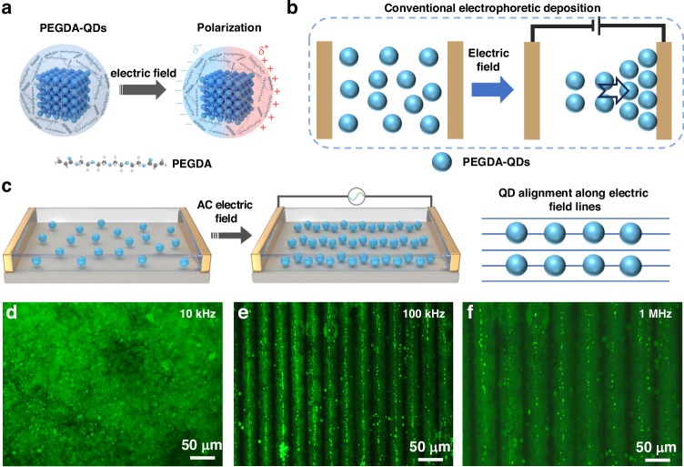
The high pixel resolution is emerging as one of the key parameters for the next-generation displays. Despite the development of various quantum dot (QD) patterning techniques, achieving ultrahigh-resolution (>10,000 pixels per inch (PPI)) and high-fidelity QD patterns is still a tough challenge that needs to be addressed urgently. Here, we propose a novel and effective approach of orthogonal electric field-induced template-assisted dielectric electrophoretic deposition to successfully achieve one of the highest pixel resolutions of 23090 (PPI) with a high fidelity of up to 99%. Meanwhile, the proposed strategy is compatible with the preparation of QD pixels based on perovskite CsPbBr3 and conventional CdSe QDs, exhibiting a wide applicability for QD pixel fabrication. Notably, we further demonstrate the great value of our approach to achieve efficiently electroluminescent QD pixels with a peak external quantum efficiency of 16.5%. Consequently, this work provides a general approach for realizing ultrahigh-resolution and high-fidelity patterns based on various QDs and a novel method for fabricating QD-patterned devices with high performance.
© 2024. The Author(s).
Conflict of interest statement
The authors declare no competing interests.
Figures


Similar articles
-
Large-area patterning of full-color quantum dot arrays beyond 1000 pixels per inch by selective electrophoretic deposition.Nat Commun. 2021 Jul 29;12(1):4603. doi: 10.1038/s41467-021-24931-x. Nat Commun. 2021. PMID: 34326332 Free PMC article.
-
Wafer-scale patterning of high-resolution quantum dot films with a thickness over 10 μm for improved color conversion.Nanoscale. 2023 Nov 23;15(45):18317-18327. doi: 10.1039/d3nr04615j. Nanoscale. 2023. PMID: 37921020
-
Freestanding High-Resolution Quantum Dot Color Converters with Small Pixel Sizes.ACS Appl Mater Interfaces. 2022 Nov 2;14(43):48995-49002. doi: 10.1021/acsami.2c14212. Epub 2022 Oct 23. ACS Appl Mater Interfaces. 2022. PMID: 36274221
-
Patterning technologies of quantum dots for color-conversion micro-LED display applications.Nanoscale. 2025 Jan 23;17(4):1764-1789. doi: 10.1039/d4nr03925d. Nanoscale. 2025. PMID: 39688022 Review.
-
Patterning Quantum Dots via Photolithography: A Review.Adv Mater. 2023 Oct;35(41):e2300546. doi: 10.1002/adma.202300546. Epub 2023 Aug 2. Adv Mater. 2023. PMID: 36892995 Review.
Cited by
-
Shadow-Assisted Sidewall Emission for Achieving Submicron Linewidth Light Source by Using Normal UV Photolithography.Nanomicro Lett. 2025 Apr 22;17(1):228. doi: 10.1007/s40820-025-01737-w. Nanomicro Lett. 2025. PMID: 40261463 Free PMC article.
-
Rigid crosslinker-assisted nondestructive direct photolithograph for patterned QLED displays.Light Sci Appl. 2025 Jul 24;14(1):251. doi: 10.1038/s41377-025-01918-7. Light Sci Appl. 2025. PMID: 40707459 Free PMC article.
-
Nanosecond response perovskite quantum dot light-emitting diodes with ultra-high resolution for active display application.Light Sci Appl. 2025 Aug 21;14(1):285. doi: 10.1038/s41377-025-01959-y. Light Sci Appl. 2025. PMID: 40841515 Free PMC article.
References
-
- Hassan, Y. et al. Ligand-engineered bandgap stability in mixed-halide perovskite LEDs. Nature591, 72–77 (2021). - PubMed
-
- Coe, S. et al. Electroluminescence from single monolayers of nanocrystals in molecular organic devices. Nature420, 800–803 (2002). - PubMed
-
- Colvin, V. L., Schlamp, M. C. & Alivisatos, A. P. Light-emitting diodes made from cadmium selenide nanocrystals and a semiconducting polymer. Nature370, 354–357 (1994).
-
- Huang, P. et al. Nonlocal interaction enhanced biexciton emission in large CsPbBr3 nanocrystals. eLight3, 10 (2023).
LinkOut - more resources
Full Text Sources
