. 2025 Jan;20(1):43-50.
doi: 10.1038/s41565-024-01792-1. Epub 2024 Sep 26.

On-demand nanoengineering of in-plane ferroelectric topologies

Affiliations

On-demand nanoengineering of in-plane ferroelectric topologies

Marti Checa et al. Nat Nanotechnol. 2025 Jan.

Abstract

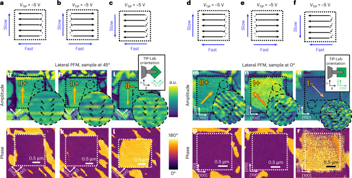
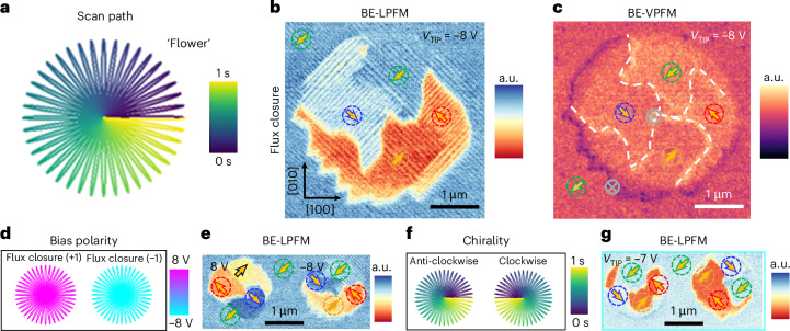
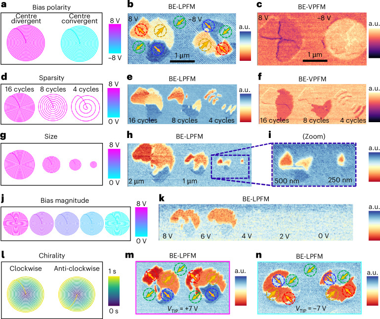
Hierarchical assemblies of ferroelectric nanodomains, so-called super-domains, can exhibit exotic morphologies that lead to distinct behaviours. Controlling these super-domains reliably is critical for realizing states with desired functional properties. Here we reveal the super-switching mechanism by using a biased atomic force microscopy tip, that is, the switching of the in-plane super-domains, of a model ferroelectric Pb0.6Sr0.4TiO3. We demonstrate that the writing process is dominated by a super-domain nucleation and stabilization process. A complex scanning-probe trajectory enables on-demand formation of intricate centre-divergent, centre-convergent and flux-closure polar structures. Correlative piezoresponse force microscopy and optical spectroscopy confirm the topological nature and tunability of the emergent structures. The precise and versatile nanolithography in a ferroic material and the stability of the generated structures, also validated by phase-field modelling, suggests potential for reliable multi-state nanodevice architectures and, thereby, an alternative route for the creation of tunable topological structures for applications in neuromorphic circuits.


Conflict of interest statement

Competing interests: The authors declare no competing interests.

Figures

Fig. 1
Fig. 1. Pristine super-domain distribution in PSTO.
a, The surface topography. b, A BE-LPFM image of the pristine sample showing the four distinct super-domain structures. The inset shows the relative TIP-laboratory orientation, the relative orientation between the cantilever of the microscope and the axes of the laboratory. c, The local (black) and global (yellow) dipole distribution for the four different super-domains (I+, I−, II+ and II−). The zoom-ins display examples of the four possible super-domains in the colour dashed circles in b.
Fig. 2
Fig. 2. Hierarchical super-switching in PSTO.
ac, Illustration of tip bias and scan paths for different slow and fast-scan directions, respectively, with the samples' main crystallographic axis at 45° relative to the laboratory axes (X, Y). VTIP is the writing bias. Inset shows the corresponding tip-laboratory orientation. df, lllustration of tip bias and scan paths for different slow and fast-scan directions, respectively, with the samples' main crystallographic axis at 0° relative to the laboratory axes (X, Y). VTIP is the writing bias. Inset shows the corresponding tip-laboratory orientation, the relative orientation between the cantilever of the microscope and the axes of the laboratory. gl, Lateral PFM amplitude (gi) and phase (jl) images post raster scanning, corresponding to the writing trajectories shown in a–c, respectively. mr, Lateral PFM amplitude (mo) and phase (pr) images post raster-scanning, corresponding to the writing trajectories shown in df. Insets in amplitude images are amplified images to visualize the superlattice direction. The time used for the fast-scan was 1 s per line which, multiplied by 128 lines, gives us 2 min and 8 s for the slow-scan to be completed.
Fig. 3
Fig. 3. Generation of centre-divergent and centre-convergent structures through spiral-scan lithography.
a, An illustration of the experimental setup used for the measurements: AEcroscopy Python package controls an FPGA, which inputs the generated signals (tip bias V(t), X piezo bias X(t) and Y piezo bias, Y(t)) to the AFM controller to autonomously perform the previously Python-designed experiment. b, BE-LPFM piezoresponse (cantilever long axis parallel to [100] crystallographic axis of the sample) of the written centre-convergent structure. c, BE-VPFM piezoresponse of the written centre-convergent structure; the grey cross and dot in a circle indicate the direction of the out-of-plane components for head to head and tail to tail. d, A spiral tip trajectory for the writing of the centre-convergent structure, starting the path at the centre and with a total duration of 1 s. e, BE-LPFM piezoresponse (cantilever long axis parallel to [100] crystallographic axis of the sample) of the written centre-divergent structure. f, BE-VPFM piezoresponse of the written centre-divergent structure; the grey cross and dot in a circle indicate the direction of the out-of-plane components for head to head and tail to tail. g, SEM-CL map of the same centre-divergent structure. h, An SHG map of the same centre-divergent structure with the polarizer at −45° (see green arrow). i, An SHG map of the same centre-divergent structure with the polarizer at +45° (see green arrow). j, Single SEM-CL spectra at head-to-head and tail-to-tail super-boundaries in the locations indicated by the black and blue dots in g, respectively. VTIP is the writing bias used to generate the structure. Int, intensity of the cathodoluminescence (CL) signal.
Fig. 4
Fig. 4. Phase-field modelling of the centre-divergent and centre-convergent structures.
a, The nanoscale arrangement of the global (orange) and local (black) ferroelectric dipoles in the in-plane directions for the four different super-domains. The colour legend indicates the three-dimensional polarization direction for the phase-field structures. b, The initial state used in the phase-field modelling for the centre-divergent structure. c, The initial state used in the phase-field modelling for the centre-convergent structure. d, The equilibrium state obtained in the phase-field modelling for the centre divergent. The inset describes the experimental BE-LPFM and BE-VPFM of the centre-divergent structures of Fig. 3. The Z-cut cross-section across the whole film along the dashed green line is shown on the right. e, The equilibrium state obtained in the phase-field modelling for the centre-convergent. The inset describes the experimental BE-LPFM and BE-VPFM of the centre-convergent structures of Fig. 3. The Z-cut cross-section across the whole film along the dashed green line is shown on the right. The colour legend indicates the three-dimensional polarization direction for the phase-field structures in-plane (IP) and out-of-plane (OP).
Fig. 5
Fig. 5. Generation of flux-closure structures through flower-scan lithography.
a, Flower tip trajectory used for the writing. b, BE-LPFM piezoresponse (cantilever long axis parallel to [100] crystallographic axis of the sample) of the written flux-closure structure. c, BE-VPFM piezoresponse of the same structure; the grey cross and dot in a circle indicate the direction of the out-of-plane components for head to head and tail to tail. d, A scan bias polarity used to write the flux-closure states with clockwise and anti-clockwise polarization rotation. e, BE-LPFM piezoresponse of the structures written using the parameters in d. f, Flower scan path structure with different chirality, starting the path at the centre and with a total duration of 1 s. g, BE-LPFM piezoresponse of the written structures with negative bias using the scan paths in f. VTIP is the writing bias used.
Fig. 6
Fig. 6. Tunability of the centre-convergent and centre-divergent states.
a, A scan bias polarity used to write the centre-divergent and centre-convergent states. b,c, BE-LPFM piezoresponse (b) and BE-VPFM piezoresponse (c) of the structures written using the parameters in a. d, Scan paths with different sparsity. e,f, BE-LPFM piezoresponse (e) and BE-VPFM piezoresponse (f) of the structures written using the parameters in d. g, A scan path with a different size. h,i, BE-LPFM piezoresponse (h) and BE-VPFM piezoresponse (i) of the structures written using the parameters in g. j, A scan path with different writing bias magnitude. k, BE-LPFM piezoresponse of the structures written using the parameters in j. l, A spiral-scan path with different chirality/handedness, starting the path at the centre and with a total duration of 1 s. m, BE-LPFM piezoresponse of the written structures with positive bias using the scan paths in l. n, BE-LPFM piezoresponse of the written structures with negative bias using the scan paths in l. VTIP is the writing bias used.

References

    1. Chen, S. et al. Recent progress on topological structures in ferroic thin films and heterostructures. Adv. Mater.33, 2000857 (2021). - PubMed
    1. Catalan, G., Seidel, J., Ramesh, R. & Scott, J. F. Domain wall nanoelectronics. Rev. Mod. Phys.84, 119 (2012).
    1. Marković, D., Mizrahi, A., Querlioz, D. & Grollier, J. Physics for neuromorphic computing. Nat. Rev. Phys.2, 499–510 (2020).
    1. Junquera, J. et al. Topological phases in polar oxide nanostructures. Rev. Mod. Phys.95, 025001 (2023).
    1. McConville, J. P. V. et al. Ferroelectric domain wall memristor. Adv. Funct. Mater.30, 2000109 (2020). - PMC - PubMed