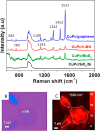
2D Material-Based Surface-Enhanced Raman Spectroscopy Platforms (Either Alone or in Nanocomposite Form)-From a Chemical Enhancement Perspective
- PMID: 39346812
- PMCID: PMC11425813
- DOI: 10.1021/acsomega.4c06398
2D Material-Based Surface-Enhanced Raman Spectroscopy Platforms (Either Alone or in Nanocomposite Form)-From a Chemical Enhancement Perspective
Abstract
Surface-enhanced Raman spectroscopy (SERS) is a vibrational spectroscopic technique with molecular fingerprinting capability and high sensitivity, even down to the single-molecule level. As it is 50 years since the observation of the phenomenon, it has now become an important task to discuss the challenges in this field and determine the areas of development. Electromagnetic enhancement has a mature theoretical explanation, while a chemical mechanism which involves more complex interactions has been difficult to elucidate until recently. This article focuses on the 2D material-based platforms where chemical enhancement (CE) is a significant contributor to SERS. In the context of a diverse range (transition metal dichalcogenides, MXenes, etc.) and categories (insulating, semiconducting, semimetallic, and metallic) of 2D materials, the review aims to realize the influence of various factors on SERS response such as substrates (layer thickness, structural phase, etc.), analytes (energy levels, molecular orientation, etc.), excitation wavelengths, molecular resonances, charge-transfer transitions, dipole interactions, etc. Some examples of special treatments or approaches have been outlined for overcoming well-known limitations of SERS and include how CE benefits from the defect-induced physicochemical changes to 2D materials mostly via the charge-transport ability or surface interaction efficiency. The review may help readers understand different phenomena involved in CE and broaden the substrate-designing approaches based on a diverse set of 2D materials.
© 2024 The Author. Published by American Chemical Society.
Conflict of interest statement
The author declares no competing financial interest.
Figures


Similar articles
-
Plasmon-Free Surface-Enhanced Raman Spectroscopy Using Metallic 2D Materials.ACS Nano. 2019 Jul 23;13(7):8312-8319. doi: 10.1021/acsnano.9b03761. Epub 2019 Jul 11. ACS Nano. 2019. PMID: 31284713
-
Surface Enhanced Raman Scattering Revealed by Interfacial Charge-Transfer Transitions.Innovation (Camb). 2020 Oct 13;1(3):100051. doi: 10.1016/j.xinn.2020.100051. eCollection 2020 Nov 25. Innovation (Camb). 2020. PMID: 34557716 Free PMC article. Review.
-
Beyond the Charge Transfer Mechanism for 2D Materials-Assisted Surface Enhanced Raman Scattering.Anal Chem. 2024 Jun 18;96(24):9917-9926. doi: 10.1021/acs.analchem.4c01051. Epub 2024 Jun 5. Anal Chem. 2024. PMID: 38837181
-
Exploring and Engineering 2D Transition Metal Dichalcogenides toward Ultimate SERS Performance.Adv Mater. 2024 May;36(19):e2312348. doi: 10.1002/adma.202312348. Epub 2024 Feb 11. Adv Mater. 2024. PMID: 38302855 Review.
-
2D GaN for Highly Reproducible Surface Enhanced Raman Scattering.Small. 2021 Nov;17(45):e2103442. doi: 10.1002/smll.202103442. Epub 2021 Sep 27. Small. 2021. PMID: 34569140
Cited by
-
Molecular spectroscopies with semiconductor metasurfaces: towards dual optical/chemical SERS.J Mater Chem C Mater. 2025 May 22;13(23):11499-11514. doi: 10.1039/d4tc05420b. eCollection 2025 Jun 12. J Mater Chem C Mater. 2025. PMID: 40417182 Free PMC article. Review.
References
-
- Fleischmann M.; Hendra P. J.; McQuillan A. J. Raman Spectra of Pyridine Adsorbed at a Silver Electrode. Chem. Phys. Lett. 1974, 26, 163–166. 10.1016/0009-2614(74)85388-1. - DOI
-
- Jeanmaire D. L.; Van Duyne R. P. Surface raman spectroelectrochemistry: Part I. Heterocyclic, aromatic, and aliphatic amines adsorbed on the anodized silver electrode. J. Electroanal. Chem. Interfacial Electrochem. 1977, 84, 1–20. 10.1016/S0022-0728(77)80224-6. - DOI
-
- Albrecht M. G.; Creighton J. A. Anomalously Intense Raman Spectra of Pyridine at a Silver Electrode. J. Am. Chem. Soc. 1977, 99, 5215–5217. 10.1021/ja00457a071. - DOI
-
- Moskovits M. Surface Roughness and the Enhanced Intensity of Raman Scattering by Molecules Adsorbed on Metals. J. Chem. Phys. 1978, 69, 4159–4161. 10.1063/1.437095. - DOI
LinkOut - more resources
Full Text Sources
Research Materials
Miscellaneous
