. 2024;1(1):11.
doi: 10.1038/s44335-024-00010-4. Epub 2024 Oct 3.

Demonstration of 4-quadrant analog in-memory matrix multiplication in a single modulation

Affiliations

Demonstration of 4-quadrant analog in-memory matrix multiplication in a single modulation

Manuel Le Gallo et al. Npj Unconv Comput. 2024.

Abstract

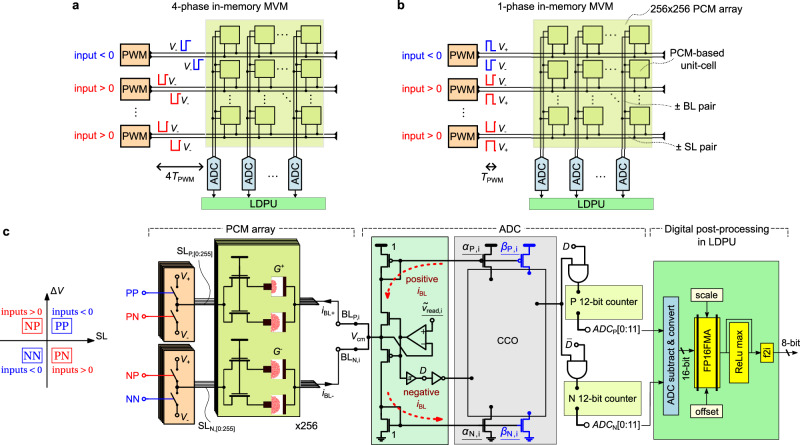
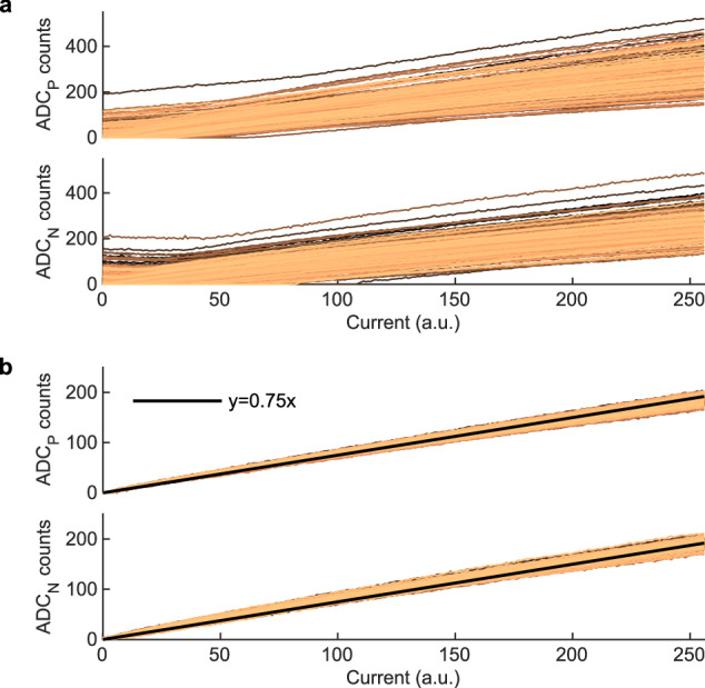
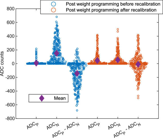
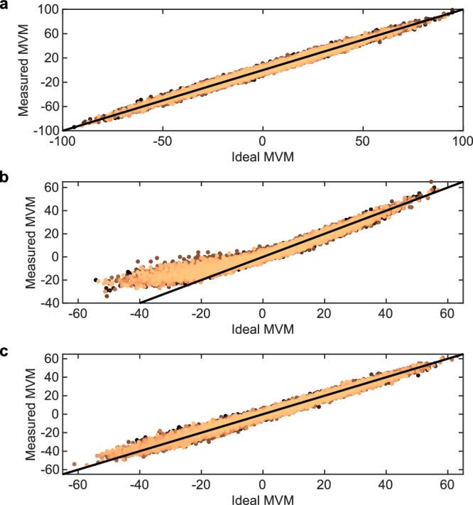
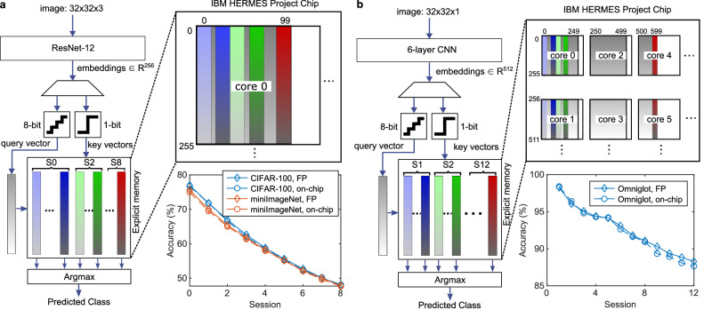
Analog in-memory computing (AIMC) leverages the inherent physical characteristics of resistive memory devices to execute computational operations, notably matrix-vector multiplications (MVMs). However, executing MVMs using a single-phase reading scheme to reduce latency necessitates the simultaneous application of both positive and negative voltages across resistive memory devices. This degrades the accuracy of the computation due to the dependence of the device conductance on the voltage polarity. Here, we demonstrate the realization of a 4-quadrant MVM in a single modulation by developing analog and digital calibration procedures to mitigate the conductance polarity dependence, fully implemented on a multi-core AIMC chip based on phase-change memory. With this approach, we experimentally demonstrate accurate neural network inference and similarity search tasks using one or multiple cores of the chip, at 4 times higher MVM throughput and energy efficiency than the conventional four-phase reading scheme.

Keywords: Electrical and electronic engineering; Electronic devices.


Conflict of interest statement

Competing interestsThe authors declare no competing interests.

Figures

Fig. 1
Fig. 1. Implementation of single-phase in-memory MVM.
a In-memory MVM in four phases. Inputs of positive and negative polarity are applied individually to weights of positive and negative polarity using a single voltage polarity (V) in four modulation cycles 4TPWM. b In-memory MVM in a single phase. Inputs of positive and negative polarity are applied simultaneously to weights of positive and negative polarity with voltages of opposite polarity (V+, V) in one modulation cycle TPWM. c Implementation of the single-phase in-memory MVM on the IBM HERMES Project Chip. The procedure is shown for a single BL of an AIMC core of the chip. ΔV refers to the voltage drop on the SL with respect to Vcm, e.g., ΔV = V+,− − Vcm. In the abbreviations for the SL connections shown on the left, the first letter refers to the SL polarity, and the second to the polarity of the read voltage applied at the bottom electrode of the PCM devices. For example, PN means connecting SLP to V. When the SL input is >0, the PN and NP switches are activated, and when it is <0, PP and NN are activated.
Fig. 2
Fig. 2. Conductance polarity dependence measurement.
a Conductance measured in negative voltage polarity as a function of conductance measured in positive voltage polarity at Vread ≃0.2 V for 130 k PCM devices of an AIMC core. The blue line is a guide to the eye that shows the average trend. In order to compare the polarity dependence of devices that have different SET conductance on the same graph, the conductance of each device is normalized by the SET conductance of that device for each polarity. The mean SET conductance of all devices is approximately 20 μS. b Low-angle annular darkfield scanning transmission electron microscope image of a fully RESET PCM device showing a substantially large amorphous region that fully blocks the bottom electrode. Electrode-amorphous and amorphous-crystalline interfaces are highlighted. c Band diagrams of the PCM device at equilibrium, under positive and negative polarity bias. Only the valence band is shown because the Ge2Sb2Te5 material is a p-type semiconductor in the amorphous phase. Schottky barriers for holes appear at both interfaces, with the barrier of the amorphous-crystalline interface greater than that of the electrode-amorphous interface. When a positive bias is applied at the top electrode with respect to the bottom electrode, the back-to-back diode configuration entails the amorphous-crystalline interface being reverse-biased and the electrode-amorphous interface forward-biased. This effect reverses when the polarity is negative. Thus, larger current flows when the dominating diode is forward-biased, which is the amorphous-crystalline interface. This occurs for the negative polarity of the applied bias, i.e., when Vcm is applied at the top electrode and V+ at the bottom electrode.
Fig. 3
Fig. 3. Initial ADC calibration.
a Positive (ADCP) and negative (ADCN) transfer curves of the 256 ADCs prior to calibration. b ADC transfer curves after calibration. The transfer curves are measured with all devices of the core programmed to the RESET state, by gradually activating one SL after the other, starting from 0 up to 256 SLs.
Fig. 4
Fig. 4. Effect of v~read,i recalibration post weight programming.
ADC values are measured when setting half of the SL inputs to a positive value and the other half to an equal in magnitude negative one after uniformly distributed weights within [−1, 1] range have been programmed in the core. The expected distribution of ADCP − ADCN values should be centered around zero, which is effectively achieved after recalibration.
Fig. 5
Fig. 5. MVM accuracy measurement results.
a 4-quadrant MVM results using the conventional four-phase reading scheme. b 4-quadrant MVM results using the single-phase reading scheme. c 2-quadrant MVM results (positive-only inputs) using the single-phase reading scheme. The black line in the plots is a y = x guide to the eye.
Fig. 6
Fig. 6. MNIST accuracy experimental results.
a Network used for MNIST handwritten digit recognition. b Implementation of the network on one core of the chip. The weights of the first and second layers are replicated 4 and 2 times, respectively, as indicated by the red borders. The inputs to those layers are also replicated the same number of times. This is done to increase the input current to the ADC and average the weight programming noise, which improves the signal-to-noise ratio and leads to higher accuracy. The last 16 SLs of the core are reserved for the bias weights (see “Implementation”). c Accuracy obtained from the on-chip experiments with four-phase and single-phase reading schemes compared with the accuracy of the same model run in software (FP model).
Fig. 7
Fig. 7. FSCL inference experiments.
a Accuracy obtained from the on-chip experiments with the single-phase reading scheme compared with the software accuracy (FP) for the inference stage of FSCL tasks on the CIFAR-100 and miniImageNet datasets. The dataset contains natural images of 100 classes in total, which are divided into a first session (S0) containing 60 classes with 200 training and 100 query examples per class, and eight subsequent sessions (S1–S8) with 5 novel classes introduced in each session containing 5 support examples and 100 query examples per class. The learned key vectors occupy 256 SLs and 60 BLs (classes) on the array in S0, evolving to 100 BLs (classes) in the last S8. b Accuracy obtained from the on-chip experiments with the single-phase reading scheme compared with the software accuracy (FP) for the inference stage of FSCL tasks on the Omniglot dataset. The dataset contains handwritten figures of 1623 characters from 50 alphabets. For FSCL evaluation we use 600 character classes from the test set organized into 12 sessions. Each session contains 50 classes, and each class consists of 5 support examples and 15 query examples. The learned key vectors are 512 dimensional and mapped across a pair of cores. The lower 256 dimensions of a key vector are mapped to all 256 SLs in one core, and the higher 256 dimensions are mapped to 256 SLs in a second core along the corresponding BLs. The 250 class vectors until the 5th session can be mapped to 250 BLs in one pair of cores (core 0, core 1). Similarly, sessions 6th to 10th can be mapped to core 2, core 3. Finally, the 11th and 12th sessions' key vectors are mapped to 100 BLs across core 4 and core 5.

References

    1. Sebastian, A., Le Gallo, M., Khaddam-Aljameh, R. & Eleftheriou, E. Memory devices and applications for in-memory computing. Nat. Nanotechnol.15, 529–544 (2020). - PubMed
    1. Huang, Y. et al. Memristor-based hardware accelerators for artificial intelligence. Nat. Rev. Electr. Eng.1, 286–299 (2024).
    1. Aguirre, F. et al. Hardware implementation of memristor-based artificial neural networks. Nat. Commun.15, 1974 (2024). - PMC - PubMed
    1. Le Gallo, M. et al. A 64-core mixed-signal in-memory compute chip based on phase-change memory for deep neural network inference. Nat. Electron.6, 680–1693 (2023).
    1. Ambrogio, S. et al. An analog-AI chip for energy-efficient speech recognition and transcription. Nature620, 768–775 (2023). - PMC - PubMed