

. 2024 Mar;11(3):10.1364/OPTICA.506108.
doi: 10.1364/OPTICA.506108.
Low-power, agile electro-optic frequency comb spectrometer for integrated sensors
Affiliations
- PMID: 39381536
- PMCID: PMC11459449
- DOI: 10.1364/OPTICA.506108
Item in Clipboard
Low-power, agile electro-optic frequency comb spectrometer for integrated sensors
Optica.
2024 Mar.
No abstract available
Figures
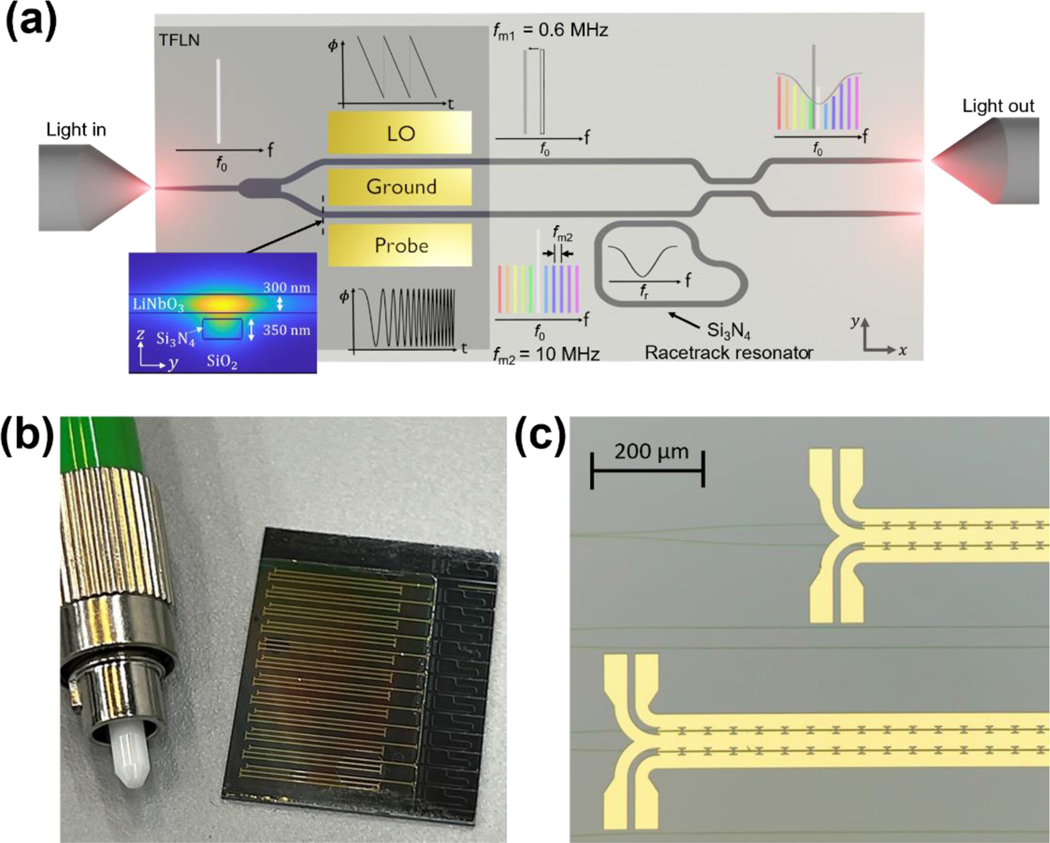
a. Schematic of the integrated electro-optic frequency comb spectrometer. The left portion of the chip (shaded area) is a bonded thin-film lithium niobate (TFLN) layer for active modulation. Input light, injected from the left lensed fiber with a carrier frequency, , is split into two arms. The lower arm (labeled as Probe) is modulated by a chirped waveform, generating an electro-optic frequency comb with a repetition rate of MHz. This comb then interrogates a given resonance, located at , of the silicon nitride racetrack resonator. The upper arm, which serves a local oscillator (LO), is modulated by a sawtooth waveform, shifting its center frequency by kHz through the serrodyne process. The probe and LO are then combined before being sent to an off-chip photodetector. The inset shows a cross-sectional view of the waveguide with the electric field intensity distribution. b. Photograph of an integrated electro-optic frequency comb spectrometer chip containing twenty-four individual electro-optic modulators and integrated temperature sensors. A fiber ferrule is shown for scale. c. Optical microscopy image of the electrode area. The capacitively loaded slow wave electrode design was used for and bandwidth measurement. The conventional unpatterned electrode design was used for the photonic readout of the two cavity-based sensors.

Performance of the fabricated devices. a. Half-wave voltage, , measurement. The normalized transmission through the interferometer (blue, left axis) approaches a near-continuous sine wave when driven with a 30 kHz triangular signal (red, right axis) at V. b. Average electro-optic response of the fabricated EOM from five repeated measurements, yielding a 3 dB bandwidth of greater than 40 GHz. The shown uncertainties are the standard error of the mean from the repeated measurements.
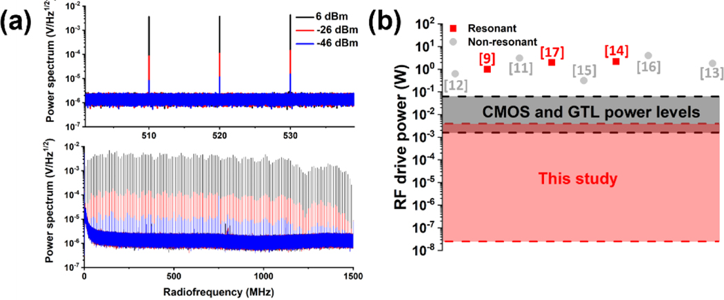
a. Photodetected power spectrum of the integrated optical frequency comb for a range of root-mean-square radiofrequency (RF) chirp powers. Comb teeth are clearly visible even at drive powers as low as 25 nW (−46 dBm). Each of the shown power spectra is the average of one hundred spectra, each of which was acquired in 10 ms. b. Comparison of the RF drive powers used in this study to those in the literature for both non-resonant (i.e., frequency-agile) and resonant (essentially fixed frequency) devices. The literature values are indicated by their corresponding reference numbers. We note the lowest RF drive power used in the present study is 71 dB lower than the lowest previously reported value while still maintaining frequency agility. Also shown are the corresponding ranges for CMOS and GTL logic levels.

On-chip racetrack resonator temperature dependence. a. Measured cavity mode shift as a function of temperature as well as a linear fit. Each data point is the average of 500 individual Lorentzian fits to 200 μs long measurements. Temperature and frequency change is referenced to measurements made at ≈ 27.1 °C. The standard error of the mean for each frequency data set was between 36 kHz and 93 kHz, leading to statistical uncertainties much smaller than the shown data point size. We observe good linearity in these measurements with the shown slope being near the calculated value of ≈ 2500 MHz/°C. b. Allan deviation of repeated measurements of the chip’s temperature made by measuring the cavity’s mode frequency and converting to temperature based on the slope determined in panel a. At ≈ 20 ms we reach a minimum of the Allan deviation of 30 μK. The inset gives the corresponding temperature change time series.

a. Schematic of the chip-scale optomechanical accelerometer (shown not to scale). The two bonded silicon chips are shown in white with the silicon nitride beams shown in dark gray. The highly reflective mirror coatings are shown in green with the anti-reflective coatings shown in blue. In the presence of acceleration, the plano-concave cavity’s length will change due to the motion of the proof mass to which the planar mirror is attached. This cavity mode displacement can be readily recorded with the on-chip optical frequency comb spectrometer (with the light shown in red). b. A stitched optical microscope image of the accelerometer showing the proof mass resonator with a planar mirror (at center) and supporting silicon nitride beams around the edge of proof mass. c. Simultaneously measured spectra of the on-chip racetrack-resonator-based temperature sensor (Temp. Sensor) and the chip-scale optomechanical acceleration sensor (Accel. Sensor). Two separate comb spectra are shown for two separate moments in time, with the upper spectrum vertically offset by 1. While the temperature sensor resonance is nominally static, the accelerometer resonance translates in the presence of acceleration. The shown comb spectra were recorded in only 200 μs with no averaging performed. The x-axis is relative to the measured wavemeter frequency of MHz. Also shown are two corresponding Lorentzian fits. d. Retrieved cavity mode positions for the two sensors when the Accel. Sensor was driven by a 9.81 m/s2 (i.e., 1 g) acceleration at a frequency of 100 Hz. Each of the shown data points was recorded in 200 μs.
References
-
- Picqué N and Hänsch TW, “Frequency comb spectroscopy,” Nat Photonics 13, 146–157 (2019).
-
- Torres-Company V and Weiner AM, “Optical frequency comb technology for ultra-broadband radio-frequency photonics,” Laser Photon Rev 8, 368–393 (2014).
-
- Parriaux A, Hammani K, and Millot G, “Electro-optic frequency combs,” Adv Opt Photonics 12, 223 (2020).
-
- Weigel PO, Zhao J, Fang K, Al-Rubaye H, Trotter D, Hood D, Mudrick J, Dallo C, Pomerene AT, Starbuck AL, DeRose CT, Lentine AL, Rebeiz G, and Mookherjea S, “Bonded thin film lithium niobate modulator on a silicon photonics platform exceeding 100 GHz 3-dB electrical modulation bandwidth,” Opt Express 26, 23728 (2018). - PubMed
-
- Mercante AJ, Yao P, Shi S, Schneider G, Murakowski J, and Prather DW, “110 GHz CMOS compatible thin film LiNbO3 modulator on silicon,” Opt Express 24, 15590 (2016). - PubMed
Grants and funding
LinkOut - more resources
Full Text Sources