. 2024 Oct 10;15(1):8788.
doi: 10.1038/s41467-024-53150-3.

Direct-bonded diamond membranes for heterogeneous quantum and electronic technologies

Affiliations

Direct-bonded diamond membranes for heterogeneous quantum and electronic technologies

Xinghan Guo et al. Nat Commun. .

Abstract

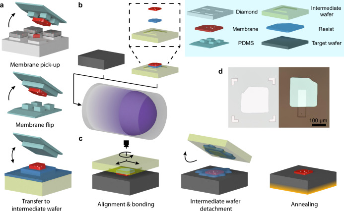
Diamond has superlative material properties for a broad range of quantum and electronic technologies. However, heteroepitaxial growth of single crystal diamond remains limited, impeding integration and evolution of diamond-based technologies. Here, we directly bond single-crystal diamond membranes to a wide variety of materials including silicon, fused silica, sapphire, thermal oxide, and lithium niobate. Our bonding process combines customized membrane synthesis, transfer, and dry surface functionalization, allowing for minimal contamination while providing pathways for near unity yield and scalability. We generate bonded crystalline membranes with thickness as low as 10 nm, sub-nm interfacial regions, and nanometer-scale thickness variability over 200 by 200 μm2 areas. We measure spin coherence times T2 for nitrogen vacancy centers in 150 nm-thick bonded membranes of up to 623 ± 21 μs, suitable for advanced quantum applications. We demonstrate multiple methods for integrating high quality factor nanophotonic cavities with the diamond heterostructures, highlighting the platform versatility in quantum photonic applications. Furthermore, we show that our ultra-thin diamond membranes are compatible with total internal reflection fluorescence (TIRF) microscopy, which enables interfacing coherent diamond quantum sensors with living cells while rejecting unwanted background luminescence. The processes demonstrated herein provide a full toolkit to synthesize heterogeneous diamond-based hybrid systems for quantum and electronic technologies.


Conflict of interest statement

X.G., A.A.H., T.D.D., A.L., I.N.H., N.D., C.T.D., and F.J.H. filed a PCT (International) patent for the methods of bonding diamond membranes.

Figures

Fig. 1
Fig. 1. Schematics of the plasma-activated bonding of diamond membranes.
a Diamond membrane transfer to the intermediate wafer. From top to down: membrane pick-up from the diamond substrate using PDMS1-stamp, membrane flipping with PDMS2-stamp, membrane placement to a photoresist or electron beam resist covered intermediate wafer. b Diamond back etching and downstream oxygen plasma treatment. Inset: the detailed layer stack of the ICP-etched intermediate wafer. c Plasma-activated membrane bonding. Left to right: membrane alignment and bonding, temperature-controlled intermediate wafer detachment, and post-bonding annealing. d Microscope images of 155-nm-thick diamond membranes bonded to a thermal oxide substrate with markers (left) and a fused silica substrate with a 5-μm-deep trench etched prior to bonding (right).
Fig. 2
Fig. 2. Characterization of the bonded membrane.
a AFM of the diamond bonding interface (the etched side) post ICP etching. Atomically flat surfaces with Rq ≤ 0.3 nm were observed in both small (200 nm by 100 nm, the upper figure) and large (10 μm by 5 μm, the lower figure) scanning areas. b Profilometry of a membrane-silicon heterostructure. The membrane region is highlighted by two dashed orange lines. The thickness of the membrane is 493.7 nm with a standard deviation of 1.1 nm. c The contact angle and XPS of diamond and sapphire pre- and post- high power plasma treatments. An increase of hydrophilicity is observed via the decrease of the contact angle, and the effect of oxygen termination is observed through the reduction of the carbon sp2 as obtained from C KLL extrapolation of the sp2/sp3 ratio and the enhancement of the sapphire-O signals as obtained from the O 1s peak quantification. d HRTEM image of a 10-nm-thick membrane bonded to a c-plane sapphire substrate. The 2 nm intermediate layer on top of diamond comes from the lack of surface control before gold deposition. e Top: the zoomed-in HRTEM image of the diamond-sapphire bonding interface, the red dashed rectangle region in d, showing a sub-0.5 nm thickness of the bonding intersection. Bottom: EDS elemental analysis across the bonding interface. f The PL map of GeV centers in a membrane bonded to a DBR mirror at 4 K. The signal-to-background ratio around the zero phonon line (ZPL) can be as high as 65, with the signal surpassing 65 kc s−1. g Hahn-echo measurements of one typical NV at room temperature showing a T2 value of 632 ± 21 μs. See Supplementary Section 5.7 for data acquisition and fitting details.
Fig. 3
Fig. 3. Nanophotonic integration with direct-bonded membranes.
a Schematics of TiO2-based (top) and diamond-based (bottom) nanophotonics on diamond membrane heterostructures. In this work fused silica (thermal oxide silicon) wafers are used as carrier wafers for the TiO2 (diamond)-based demonstrations. The grating couplers for excitation (collection) are colored in red (blue), respectively. b Microscope images of TiO2 fishbone cavities and ring resonators on a 50 nm-thick diamond membrane. Images were taken at the same location but different fabrication rounds. c The transmission spectrum of a fishbone cavity with resonant frequency at 737.26 nm. Inset: the transmission of the cavity with a tunable laser as the excitation source, showing a quality factor Q of 10640 ± 118. d The bright field and dark field microscope images of the ICP-etched diamond ring resonators on a thermal oxide silicon substrate, showing great uniformity with minimal process contamination. e The transmission spectrum of the diamond-based ring resonator measured at the drop port. Insets: the TE mode profile, and the TE cavity resonance with a quality factor QTE of 21883 ± 6284. The fluctuation in the right inset is caused by the instability of the optical setup.
Fig. 4
Fig. 4. Imaging of NV centers and surface-attached target molecules and cells in a flow channel.
a Widefield fluorescence microscopy image of a diamond membrane corner containing NV centers at room temperature. Only a round area in the center was illuminated to avoid back-reflection from membrane edges. b The zoomed-in image of the boxed region shown in a post rotation. c A confocal scan of the same region as b using a separate setup at room temperature. Emitters confirmed to be (not) NV centers are highlighted in cyan circles (yellow boxes). Same symbols are used in b. d A representative CW-ODMR spectrum from the NV center labeled with a white arrow in c. Additional studies of NV spin coherence are included in the Supplementary Section 5.7. e, f Widefield fluorescence microscopy images of (e) Alexa-488-labeled streptavidin protein and (f) streptavidin-conjugated Qdot-525 quantum dots that were immobilized at the same region shown in a via biotinylated surface functionalization. g Schematic illustration of the flow channel structure and a cell illuminated by total internal reflection through the diamond membrane. Fluorescence microscopy images of Alexa-488-labeled TLR2 receptors on RAW cell surfaces, under (h) episcopic and (i) objective-based TIRF illumination. Edges of the diamond membrane are also visible in these images.

References

    1. Abobeih, M. H. et al. One-second coherence for a single electron spin coupled to a multi-qubit nuclear-spin environment. Nat. Commun.9, 1 (2018). - PMC - PubMed
    1. Sukachev, D. D. et al. Silicon-Vacancy Spin Qubit in Diamond: A Quantum Memory Exceeding 10 ms with Single-Shot State Readout. Phys. Rev. Lett.119, 1 (2017). - PubMed
    1. Bernien, H. et al. Heralded entanglement between solid-state qubits separated by three metres. Nature497, 86 (2013). - PubMed
    1. Debroux, R. et al. Quantum Control of the Tin-Vacancy Spin Qubit in Diamond. Phys. Rev. X11, 41041 (2021).
    1. Abobeih, M. H. et al. Atomic-scale imaging of a 27-nuclear-spin cluster using a quantum sensor. Nature576, 411 (2019). - PubMed

LinkOut - more resources